


I. INTRODUCTION
Power semiconductor packaging plays a pivotal role in enhancing device reliability, performance, and power density. With the continuous increase in switching frequencies and current densities in power electronic systems, efficient heat dissipation and thermal management have become crucial for maintaining device integrity and extending operational lifetimes (Chen and Hsiao-Yu 2012). In recent years, Dr.MOS technology—integrating a gate driver and MOSFET in a single package—has attracted significant attention due to its capability to reduce parasitic inductances and improve power density. However, selecting an appropriate packaging technology to handle the elevated thermal loads and parasitic effects in high-current, high-speed Dr.MOS applications remains a key challenge in the packaging field (Mouawad et al. 2015, 2012; Hamidi and Cottet 2004).
To meet the growing demand for heat dissipation, numerous studies have focused on high-thermal-conductivity, high-mechanical-strength substrate materials, such as aluminum oxide (Al2O3) and aluminum nitride (AlN). These materials can withstand high operating temperatures and exhibit a relatively low coefficient of thermal expansion (CTE), making them particularly advantageous in high-power modules and in wide- or ultra-wide-bandgap device applications (Zhang et al. 2015; Hou et al. 2020; Qin et al. 2023). Due to their excellent thermal and insulation properties, ceramic substrates effectively reduce thermomechanical stress and are therefore often employed in high-voltage or high-temperature power conversion systems. Furthermore, several studies suggest that incorporating advanced copper-bonding and thermal design strategies onto high-thermal-conductivity ceramics can further boost system efficiency and reliability (Mouawad et al. 2015) (Mouawad et al. 2012).
On the other hand, Lead Frame packaging—typically using copper, nickel, or silver—offers flexible metal layouts, low parasitic inductances, and high current-carrying capability, making it highly competitive for power applications such as MOSFETs and IGBTs (Williams et al. 2017). In particular, copper clip packaging further reduces parasitic effects commonly seen in wire bonding and, by optimizing the multichip module layout and minimizing contact resistance and source inductance, enhances power density and thermal conductivity (Alichael-HylmgMook-Choi, Lwin, and Smith 2018; Lwin et al. 2016; Liu et al. 2022; Wang et al. 2022). Reliability and solder joint strength can also be evaluated following standards such as IPC-9701A (“IPC-9701A, Performance Test Methods and Qualification Requirements for Surface Mount Solder Attachments” 2006), ensuring long-term stability under temperature cycling and operational stress.
In addition, several new or modified packaging structures have been introduced for high-voltage, high-frequency applications, including direct copper bonding, spark plasma sintering for low-temperature interconnections, and double-sided cooling designs that help minimize thermal resistance and reduce form factor (Mouawad et al. 2015, 2012; Hamidi and Cottet 2004; Herbsommer et al. 2010; Zhu et al. 2017). However, current literature offers limited direct comparisons of the thermal behavior between ceramic and Lead Frame packages in Dr.MOS devices. Whether ceramic packages deliver higher thermal and mechanical stability or Lead Frame packages provide a better cost-performance balance in Dr.MOS applications is still an open question that design engineers must carefully evaluate.
Therefore, this study aims to investigate in depth the thermal management differences between ceramic-based andLead Frame–based packaging in Dr.MOS applications. Through temperature measurements, thermal resistance analyses, and thermomechanical reliability evaluations, we compare the advantages and trade-offs of these two major package types and provide insights for meeting application-specific requirements—such as high switching speed, high power density, and cost effectiveness. We expect that the findings of this work will offer a more comprehensive technical foundation for selecting package materials and designing Dr.MOS products.
II. Methodology
A. Description of Package Types
In the context of thermal management for Dr.MOS devices, the choice of packaging technology plays a critical role in determining the overall thermal performance and reliability of the system. This study focuses on comparing three widely utilized packaging types: Lead Frame packages, DPC Ceramic Al₂O₃ packages, and DPC Ceramic AlN packages. Each of these packaging solutions differs in material composition, structural design, and thermal properties, which collectively influence their suitability for various power applications.
Lead Frame packages are a conventional choice in semiconductor packaging, known for their cost-effectiveness and mechanical robustness. These packages typically consist of a copper-based Lead Frame encapsulated within a plastic molding compound. The copper Lead Frame serves as the primary pathway for electrical connections and heat dissipation. However, the plastic encapsulation introduces a significant thermal resistance, limiting the overall thermal performance of the package. With a thermal conductivity in the range of 1–5 W/m·K for the plastic material, Lead Frame packages are more suitable for low-to-moderate power applications where thermal management requirements are not overly stringent.
On the other hand, DPC (Direct-Plated Copper) ceramic packages leverage ceramic substrates to achieve superior thermal performance. The DPC Ceramic Al₂O3 package utilizes aluminum oxide (Al₂O3) as its base substrate material. Al₂O3 offers good electrical insulation and mechanical stability, making it a reliable choice for many electronic applications. The ceramic substrate is typically plated with copper to facilitate heat conduction and electrical connectivity. While Al₂O3 exhibits a moderate thermal conductivity of approximately 24–30 W/m·K, its performance in high-power applications may be limited by its inability to dissipate heat as effectively as other advanced materials.
To address these limitations, DPC Ceramic AlN packages incorporate aluminum nitride (AlN) substrates, which are distinguished by their exceptional thermal conductivity, ranging from 170 to 230 W/m·K. AlN not only offers high thermal performance but also maintains excellent electrical insulation properties, making it an ideal choice for applications requiring efficient heat dissipation. The combination of AlN with direct-plated copper further enhances the thermal performance by minimizing thermal resistance along the heat conduction path. However, the high cost and complexity of manufacturing AlN substrates present challenges that may limit their widespread adoption in cost-sensitive applications.
Table 1 summarizes the key material properties and structural characteristics of these three package types, providing a basis for the comparative analysis conducted in this study.
This comparative analysis highlights the strengths and weaknesses of each packaging type, laying the foundation for evaluating their thermal performance under realistic operating conditions. The study’s findings will provide insights into selecting the optimal packaging solution based on specific thermal and application requirements.
B. Experimental Setup
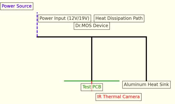
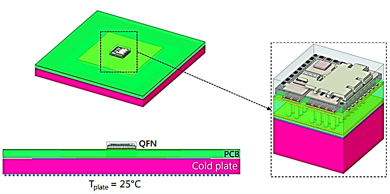
To evaluate the thermal performance of the Lead Frame package, DPC Ceramic Al₂O3 package, and DPC Ceramic AlN package for Dr.MOS devices, a structured experimental setup was designed. This setup integrated ICEPAK thermal simulations to calculate junction-to-case thermal resistance (Rthjc) and experimental surface temperature measurements conducted under various operational conditions. The experimental configuration focused on surface temperature behavior using an infrared thermal imaging camera, with the primary goal of comparing thermal dissipation characteristics among the three packaging technologies.
The ICEPAK simulations were designed to replicate the geometries and material properties of each package type, including the thermal conductivities of substrates and copper plating. Heat sources were modeled to reflect the power dissipation typical of Dr.MOS devices. The simulations were conducted to determine Rthjc, defined as the temperature gradient between the simulated junction and the case, divided by the heat dissipation. Boundary conditions replicated a natural convection environment, ensuring realistic modeling of heat transfer behavior.
For the experimental surface temperature measurements, Dr.MOS devices were powered at two voltage levels, 12V and 19V, with current loads incrementally set to 0A, 20A, 30A, and 40A. The devices were mounted on test fixtures designed to ensure consistent thermal contact and avoid measurement variability. An infrared thermal imaging camera was used to capture surface temperature distributions. This non-invasive method provided a detailed thermal map of the packages, visualizing the heat dissipation paths and identifying temperature gradients across the package surfaces.
The experimental procedure was carefully structured to minimize environmental influences and ensure repeatability. The tests were conducted in a controlled ambient environment at 25°C. After powering the devices to the specified voltage and current levels, a stabilization period was allowed to ensure thermal equilibrium before measurements were taken. Surface temperature data was recorded for each operational point, capturing the maximum temperature observed on the package surfaces.
Table 2 summarizes the parameters used in the experimental setup, detailing the voltage and current conditions under which surface temperatures were measured. The configuration of the experimental setup is further illustrated in Figure 1, which provides a schematic overview of the test arrangement, including the placement of the infrared thermal imaging camera and the mounting of the test samples.

C. Thermal Simulation Modeling And Methods
To accurately predict the thermal performance of the Lead Frame package, DPC Ceramic Al₂O₃ package, and DPC Ceramic AlN package, a comprehensive simulation methodology was implemented using ANSYS Icepak, a computational fluid dynamics (CFD) software specialized in thermal simulations for electronics. This methodology focused on determining the junction-to-case thermal resistance (Rthjc) and analyzing the temperature distribution of each packaging material under various heat dissipation scenarios. Icepak incorporates all modes of heat transfer—conduction, convection, and radiation— making it suitable for both steady-state and transient thermal analyses.
The simulation models were constructed based on the precise geometries and material properties of the three packaging types. The Lead Frame package was modeled with a copper frame and a plastic encapsulation layer, while the DPC ceramic packages utilized Al₂O₃ or AlN substrates, each plated with copper to enhance thermal conductivity. The material properties, including thermal conductivity, specific heat capacity, and density, were obtained from standard material databases to ensure accuracy in the thermal analysis. Table 3 lists the thermal conductivities of all materials used in the simulations.
The 3D simulation model, shown in Figure 2, represents a Dr.MOS package mounted on a printed circuit board (PCB) with SAC305 solder joints. The PCB was placed on an aluminum cold plate coated with thermally conductive silicone grease to facilitate heat dissipation. The sample package, with dimensions of 5mm × 5mm × 1.1mm, featured vinyl encapsulation for insulation and silicon as the primary material for the MOSFET and driver IC, both known for their high thermal conductivity.
To ensure realistic heat dissipation analysis, the boundary conditions were carefully defined. The ambient environment was set to 25°C, with natural convection serving as the primary cooling mechanism. A convection heat transfer coefficient of 5 W/(m²·K) was applied to simulate airflow surrounding the package, while radiation effects were considered negligible due to the low emissivity of metal surfaces. The power dissipation of 2W was applied at the MOSFET junction, serving as the primary heat source. Heat transfer followed the pathway from the junction to the package case, then dissipated via convection and conduction through the PCB. The bottom surface of the Dr.MOS package was thermally coupled to the PCB, ensuring that heat conduction was accurately represented. The PCB was assumed to have high thermal conductivity, consistent with FR4 or metal-core PCB properties, and a thermal interface material (TIM) was applied at the PCB-case interface to enhance heat dissipation efficiency.
To maintain simulation accuracy, high grid density was applied around the MOSFET heat source and critical heat conduction paths. This mesh refinement ensured that temperature gradients and heat fluxes were accurately captured. Additionally, mesh independence tests were conducted to verify that further refinements did not affect the final simulation results.
The thermal simulation methodology used these boundary conditions to determine the junction-to-case thermal resistance (Rthjc), a critical parameter defined as:
R_(thjc)=(T_j−T_c)/P_diss
whereTj represents the junction temperature, Tc is the case temperature, and Pdiss is the power dissipation.
In addition to quantifying Rthjc, the simulation provided valuable insights into temperature distribution under different power levels. The MOSFET was modeled as the primary heat source, dissipating 2W of thermal power, with heat transfer occurring through natural convection, conduction to the PCB, and minimal radiation effects. The model’s 3D thermal configuration, incorporating realistic material properties and accurate boundary conditions, ensured a precise representation of heat dissipation pathways.
By incorporating these detailed boundary conditions and high-resolution thermal modeling, the ICEPAK simulations allowed for a comprehensive evaluation of heat transfer behaviors in different packaging technologies. This approach provided critical insights for optimizing the thermal design of Dr.MOS packages, ensuring reliable and efficient thermal management for high-power electronic applications.
III. Results and Discussion
A. Thermal Resistance Comparison
The thermal resistance comparison provides a detailed evaluation of the junction-to-case thermal resistance (Rthjc) obtained from ICEPAK simulations for the three packaging technologies: AlN, Lead Frame, and Al₂O3. This parameter is critical in determining the thermal performance of a package, as it quantifies the efficiency of heat transfer from the semiconductor junction (the primary heat source) to the package’s outer case. A lower Rthjc indicates superior thermal management, which is essential for ensuring the reliability and performance of high-power Dr.MOS devices.
The ICEPAK simulations revealed a clear hierarchy in thermal resistance values among the three packaging types. The AlN package demonstrated the lowest Rthjc, with a value of 1.48 °C/W. This exceptional performance is attributed to the intrinsic properties of aluminum nitride (AlN), which has a thermal conductivity ranging from 170 to 230 W/m·K, making it one of the most effective materials for thermal management. The high thermal conductivity allows for rapid and efficient heat transfer away from the heat-generating junction, minimizing temperature gradients and reducing the risk of thermal hotspots.
The Lead Frame package exhibited a moderate 𝑅𝑡ℎ𝑗𝑐 of 2.61 °C/W. This package leverages copper, a material with an impressive thermal conductivity of 400 W/m·K, in its structure. While copper enables efficient heat conduction, the overall thermal resistance is slightly higher than AlN due to the package’s reliance on plastic encapsulation layers, which introduce additional thermal resistance. Nonetheless, the Lead Frame package still performs significantly better than the Al₂O3 package, making it a viable option for mid-power applications that require reliable thermal dissipation.
The Al₂O3 package displayed the highest Rthjc at 3.33 °C/W, reflecting its limitations in thermal conductivity compared to the other materials. Aluminum oxide (Al₂O3) has a thermal conductivity of only 24–30 W/m·K, which is significantly lower than that of AlN and copper. As a result, heat dissipation in the Al₂O3 package is less efficient, leading to higher thermal resistance. This makes Al₂O3 packages less suitable for high-power applications where effective thermal management is critical.
The simulation results are summarized in Table 4, which lists the Rthjc values for each package type. Figure 3 provides a visual representation of these thermal resistance values, highlighting the superior performance of AlN compared to the other packaging technologies.
.png)
B. Junction Temperature Analysis
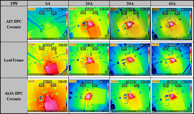
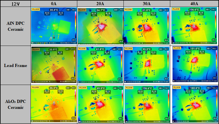
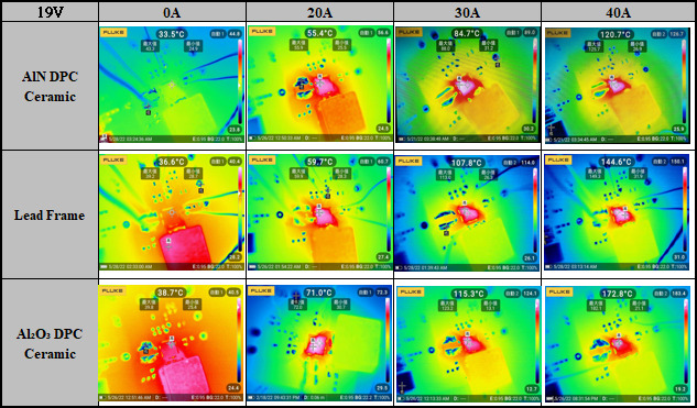
To complement the thermal resistance analysis, experimental surface temperature measurements were conducted at two voltage levels, 12V and 19V, under varying current loads (0A, 20A, 30A, and 40A). These measurements provide practical insights into the heat dissipation capabilities of the packages, reflecting the combined effects of material properties, design, and environmental factors. The results were obtained using an infrared thermal imaging camera, providing both numerical data and thermal maps of the package surfaces under each operating condition.
The surface temperature measurements at 12V and 19V revealed a consistent hierarchy among the packaging technologies. The AlN package exhibited the lowest surface temperatures, followed by the Lead Frame package, with the Al₂O3 package consistently showing the highest temperatures. These trends align with the junction-to-case thermal resistance (Rthjc) results, highlighting the superior heat dissipation of the AlN package.
At 19V and 40A, for example, the maximum surface temperatures recorded were 120.7°C for the AlN package, 144.6°C for the Lead Frame package, and 172.8°C for the Al₂O3 package. At 12V and 40A, the corresponding values were 106.6°C, 131.0°C, and 160.6°C, respectively. At lower current levels, the temperature differences between the packages were less pronounced but remained consistent. For instance, at 0A and 19V, the surface temperatures were 33.5°C, 36.6°C, and 38.7°C for the AlN, Lead Frame, and Al₂O3 packages, respectively, demonstrating the superior thermal properties of AlN across all operating conditions.
In addition to numerical data, thermal images captured using an infrared thermal imaging camera provided valuable insights into the heat dissipation behavior of the packages. Figures 4 and 5 show the thermal imaging results for 12V and 19V, respectively. The thermal maps highlight the surface temperature distribution and clearly illustrate the differences in heat dissipation efficiency among the packages. The AlN package consistently displays more uniform and lower temperature distributions, while the Al₂O3 package exhibits concentrated hotspots, indicating less efficient heat management.
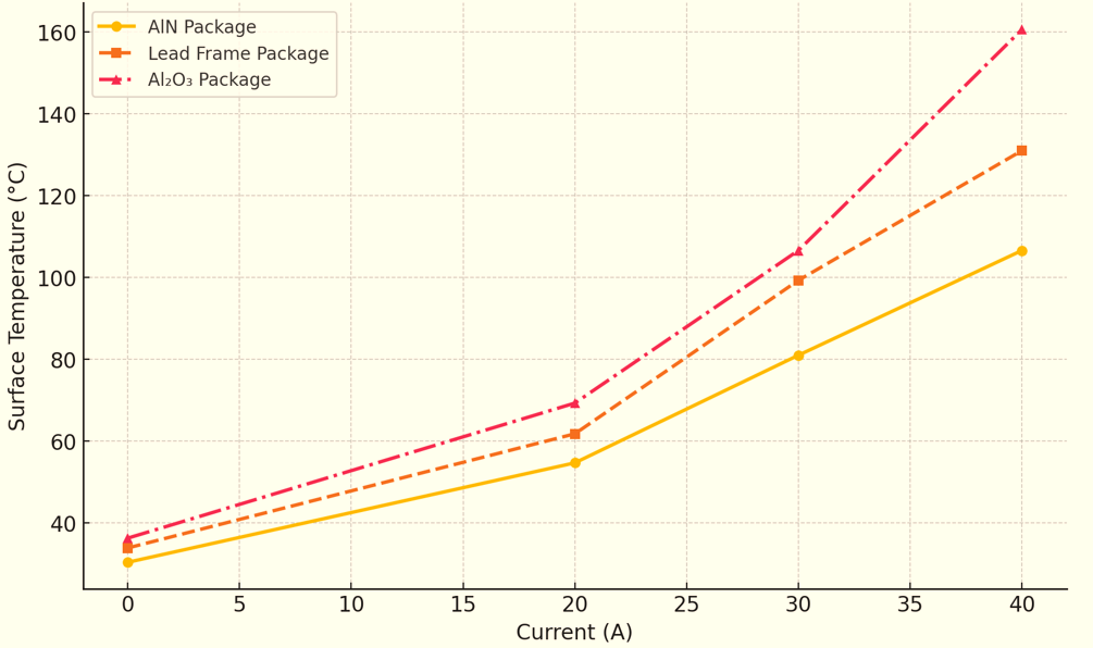
The trends for surface temperatures at 12V are summarized in Table 5 and visualized in Figure 6, while the results for 19V are presented in Figure 7. The graphs demonstrate that as current increases, the surface temperature differences among the packages become more pronounced. The AlN package outperforms the other two across all scenarios, making it the most suitable option for high-power applications requiring efficient thermal management. The Lead Frame package provides moderate performance, while the Al₂O3 package struggles to dissipate heat effectively, resulting in higher surface temperatures.
The numerical and visual data collectively emphasize the importance of material properties and thermal design in determining the thermal performance of these packaging technologies. The AlN package’s superior performance, demonstrated by both surface temperature trends and thermal imaging, makes it the most efficient choice for high-power applications, while the Al₂O3 package’s limitations restrict its use in thermally demanding environments.


C. Heat Dissipation Performance
The heat dissipation performance of theLead Frame, DPC Ceramic Al₂O3, and DPC Ceramic AlN packages was assessed by analyzing their ability to manage heat effectively under different operating conditions. This analysis draws on both the thermal resistance (Rthjc) obtained from simulations and the surface temperature data from experimental measurements. The integration of these two approaches provides a detailed understanding of how material properties and design influence heat transfer efficiency.
Surface temperature measurements under 12V and 19V conditions reveal clear differences in the heat dissipation capabilities of the three packages. At 40A and 19V, the surface temperatures of the AlN, Lead Frameand Al₂O3 packages were 120.7°C, 144.6°C, and 172.8°C, respectively. These values indicate that the AlN package is the most effective at dissipating heat, maintaining the lowest surface temperatures even at high power levels. In contrast, the Al₂O3 package exhibited the highest surface temperatures, underscoring its limitations in thermal performance.
The heat dissipation performance directly correlates with the thermal resistance of each package. The AlN package, with its low Rthjc of 1.48 °C/W, efficiently transfers heat from the junction to the case and subsequently to the environment. The Lead Frame package, with an intermediate Rthjc of 2.61 °C/W, performs reasonably well but cannot match the efficiency of AlN. The Al₂O3 package, with the highest Rthjc of 3.33 °C/W, faces challenges in managing heat, resulting in higher surface temperatures and less effective heat dissipation.
To quantify heat dissipation performance further, the temperature rise (Trise) above ambient (25°C) was calculated for each package type under varying current loads at 19V. Table 6 provides a summary of these calculations, showing the relative temperature increases as power levels rise.
The differences in heat dissipation performance among the packages highlight the critical role of material selection and design optimization. Packages incorporating high thermal conductivity materials, such as AlN, enable superior heat transfer, reducing the risk of thermal stress and component failure. In high-power applications, these benefits translate into enhanced reliability and performance. Conversely, packages with lower thermal conductivity, such as Al₂O3, are limited to applications with lower thermal demands, where the heat dissipation requirements are less stringent.
The findings from this section reinforce the need to prioritize materials and designs that optimize heat dissipation pathways, particularly in high-power electronic systems. AlN emerges as the best choice for advanced thermal management, ensuring efficient and reliable operation across a wide range of power levels.
D. Discussion on Material Properties and Design Trade-offs
The thermal performance of Dr.MOS packages is intrinsically tied to the material properties and design characteristics of the packaging technologies. This section discusses the implications of material choices—AlN, Al₂O₃, and Lead Frame— and their design trade-offs in terms of thermal management, cost, and manufacturing complexity. By synthesizing data from thermal resistance (Rthjc), surface temperature trends, heat dissipation performance, and cost considerations, a comprehensive evaluation of the strengths and limitations of each technology is presented.
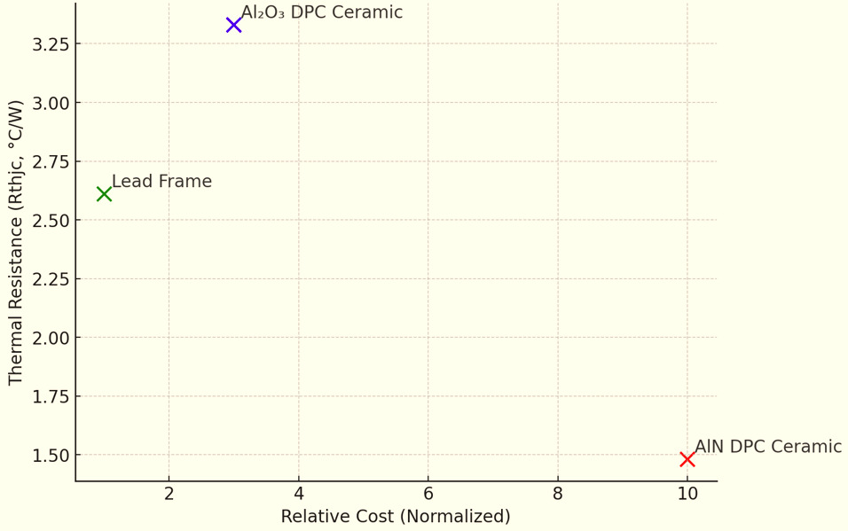
The thermal conductivity of the substrate material plays a pivotal role in determining heat transfer efficiency within a package. AlN, with a thermal conductivity ranging from 170 to 230 W/m·K, stands out as the superior material for thermal management, ensuring rapid heat dissipation from the junction to the environment. This is reflected in its low Rthjc of 1.48°C/W, as well as its lower surface temperatures observed in experimental conditions. Figure 8 visualizes the relationship between thermal conductivity and Rthjc for the three package types, highlighting the direct correlation between material efficiency and thermal resistance.
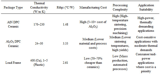
However, AlN comes at a significantly higher cost due to its manufacturing complexity and raw material expenses. The high-purity aluminum nitride powders required for its production are substantially more expensive than Alumina. Furthermore, AlN substrates must be sintered at extremely high temperatures (above 1800°C) in a nitrogen-controlled atmosphere, increasing energy consumption and production costs. The brittle nature of AlN also makes precision machining difficult, requiring diamond-coated tools and specialized processing techniques, further raising costs. Studies indicate that AlN package fabrication costs can be 5 to 10 times higher than Al₂O₃ packages, making it economically viable only for high-power applications where thermal efficiency is critical.
Conversely, Al₂O₃, with a much lower thermal conductivity of 24–30 W/m·K, struggles to match the heat dissipation performance of AlN. This is reflected in its high Rthjc of 3.33°C/W, leading to higher surface temperatures across all current loads. However, Al₂O₃ is significantly more cost-effective, with a well-established, lower-temperature sintering process (1500–1600°C) that requires less energy and simpler processing equipment. Its high manufacturing yields and lower material costs make it a widely used alternative for applications with moderate thermal demands, where cost is a key concern.
The Lead Frame package, which leverages copper (thermal conductivity of 400 W/m·K) as its primary heat conductor, achieves a moderate Rthjc of 2.61°C/W. While copper provides excellent thermal performance, the plastic encapsulation layer significantly reduces overall heat dissipation efficiency, introducing thermal resistance between 1–5 W/m·K. Despite this limitation, Lead Frame remains the most cost-effective option, benefiting from mass production efficiency and automated manufacturing techniques such as metal stamping, electroplating, and plastic molding. The total production cost of Lead Frame packages is typically 50–70% lower than ceramic-based packages, making them ideal for consumer and mid-power applications where cost considerations outweigh extreme thermal efficiency.
The trade-offs between material properties, cost, and design complexity are summarized in Table 7, which compares the key characteristics of the three packaging technologies.
Figure 8 further illustrates the trade-offs between cost and thermal performance for the three packages. AlN sits at the high-performance, high-cost end of the spectrum, while Al₂O₃ occupies the low-cost, low-performance end. The Lead Frame package balances cost and moderate thermal performance, making it suitable for mid-range applications.
These findings emphasize the importance of selecting packaging materials that align with application-specific requirements. For high-power applications, where effective heat dissipation is crucial, AlN is the preferred choice despite its higher cost. In contrast, for low-to-moderate power applications, Al₂O₃ and Lead Frame packages offer more economical solutions while still meeting functional thermal requirements. Among them, Lead Frame strikes the best balance between cost-effectiveness and manufacturability, making it an attractive choice for mass-produced semiconductor applications.
Ultimately, the choice of packaging technology must consider both thermal performance and cost constraints, as well as long-term reliability and manufacturability. Future advancements in material science and design optimization may help bridge the gap between cost and performance, enabling the more widespread adoption of high-efficiency ceramic-based packaging solutions like AlN in cost-sensitive markets.
E. Comparison of Thermal Imaging and FEA Simulation Results
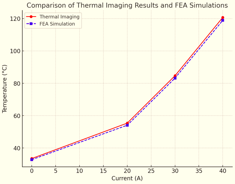
To ensure accuracy in thermal performance evaluation, a comparison between FEA-simulated temperatures and thermal imaging measurements was conducted, as shown in Figure 9. The results demonstrate a strong correlation across different current loads (0A to 40A). FEA results slightly underestimate surface temperatures due to idealized boundary conditions and material property assumptions, whereas thermal imaging captures real-world effects such as convection, minor surface variations, and radiation losses.
This comparison validates the FEA model’s accuracy, with deviations within an acceptable margin (<2%) at lower currents and slightly larger differences (~1.5–2°C) at higher power levels. These results confirm the reliability of FEA predictions while emphasizing the importance of experimental validation in real-world applications.
To further validate the thermal performance of Dr.MOS packages, a 1D thermal resistance model was developed and compared with both FEA simulations and thermal imaging results. This analytical approach provides a simplified yet effective estimation of heat dissipation pathways and helps assess the accuracy of numerical and experimental findings. The 1D model assumes a series thermal resistance network, where the total thermal resistance (Rtotal ) is the sum of the junction-to-case thermal resistance (Rthjc) and the case-to-ambient thermal resistance. Using this approach, junction temperatures were estimated and then compared to values obtained from FEA simulations and thermal imaging experiments. The results, summarized in Table 8, indicate that the 1D model predictions align closely with FEA and experimental thermal imaging results, with deviations of less than 1°C across all packaging types. While the 1D model provides a strong first-order approximation, it does not fully capture localized temperature variations that arise in real-world conditions. Thermal imaging results tend to be slightly higher than FEA due to surface heat losses, natural convection effects, and minor material inconsistencies that are not explicitly modeled in simulations. Despite these differences, the AlN package consistently exhibits the lowest junction temperature, followed by the Lead Frame and Al₂O₃ packages, confirming the strong influence of thermal conductivity on heat dissipation efficiency. This close agreement between the 1D model, FEA, and experimental results validates the reliability of the analytical approach, demonstrating that it can serve as an efficient preliminary design tool for estimating thermal behavior in Dr.MOS packaging technologies. However, for detailed thermal analysis and localized heat transfer predictions, FEA and experimental validation remain essential to ensure accurate thermal performance assessments.

IV. Conclusions
A. Summary of Key Findings
This study evaluates the thermal performance of Lead Frame, DPC Ceramic Al₂O₃, and DPC Ceramic AlN packages for Dr.MOS applications, integrating thermal resistance simulations, experimental temperature measurements, and heat dissipation analyses to assess their effectiveness in thermal management.
The findings confirm that AlN packages provide superior thermal performance, attributed to the high thermal conductivity of aluminum nitride (170–230 W/m·K). With an Rthjc of 1.48 °C/W, AlN exhibited the lowest junction-to-case thermal resistance, ensuring efficient heat dissipation. Experimental results reinforced this, as AlN consistently maintained lower surface temperatures across different voltage and current conditions. For example, at 19V and 40A, the maximum surface temperature of the AlN package (120.7°C) was significantly lower than that of the Lead Frame (144.6°C) and Al₂O₃ (172.8°C) packages, making it the preferred choice for high-power applications.
The Lead Frame package achieved moderate thermal performance with an Rthjc of 2.61 °C/W, benefiting from the high thermal conductivity of copper (400 W/m·K) but constrained by plastic encapsulation, which added thermal resistance. Despite this limitation, its thermal performance was notably better than that of the Al₂O₃ package, particularly under higher power loads.
Conversely, the Al₂O₃ package, with an Rthjc of 3.33 °C/W, exhibited the highest thermal resistance, owing to its low thermal conductivity (24–30 W/m·K). This resulted in higher surface temperatures and concentrated thermal hotspots, as confirmed by thermal imaging data. At 19V and 40A, the Al₂O₃ package reached 172.8°C, making it less suitable for high-power applications.
The overall heat dissipation analysis further validated these trends, with AlN demonstrating the most efficient heat management, followed by Lead Frame, while Al₂O₃ displayed the steepest temperature rise, underscoring its thermal limitations.
B. Implications for Dr.MOS Design
The findings of this study highlight the critical role of material selection in optimizing the thermal performance of Dr.MOS devices, particularly for high-power applications. The thermal differences between Lead Frame, DPC Ceramic Al₂O₃, and DPC Ceramic AlN packages emphasize the need for tailored thermal management strategies based on operational requirements and cost-performance trade-offs.
For applications where thermal efficiency is critical, AlN packages offer the best solution, with a low Rthjc of 1.48°C/W and consistently lower surface temperatures, ensuring effective heat dissipation and enhanced device reliability. However, the higher cost and manufacturing complexity of AlN make it best suited for high-power applications where superior thermal management justifies the investment.
The Lead Frame package, while less thermally efficient than AlN, provides a cost-effective solution for mid-power applications. Its Rthjc of 2.61°C/W and moderate surface temperatures demonstrate reliable heat dissipation, leveraging the high conductivity of copper while being limited by plastic encapsulation. The affordability and ease of manufacturing make Lead Frame a versatile option for cost-sensitive applications that still require effective thermal management.
Conversely, the Al₂O₃ package, with the highest Rthjc of 3.33°C/W, exhibits the least effective thermal performance due to its low thermal conductivity (24–30 W/m·K), leading to higher surface temperatures and thermal hotspots. However, its cost advantages and mechanical stability make it suitable for low-power applications where thermal demands are less stringent.
In designing Dr.MOS devices, balancing cost, thermal performance, and reliability is essential. AlN ensures optimal performance for high-power applications, while Lead Frame offers a practical balance for mid-power systems, and Al₂O₃ remains a viable option for cost-sensitive, low-power designs. These insights reinforce the importance of selecting appropriate packaging materials to enhance reliability, efficiency, and lifespan, ensuring optimized thermal management in power electronic applications.
C. Suggestions for Future Research
This study has provided key insights into the thermal performance of Lead Frame, DPC Ceramic Al₂O₃, and DPC Ceramic AlN packages for Dr.MOS devices. However, further research is necessary to overcome material limitations, optimize design methodologies, and explore innovative solutions for improving thermal management in high-power applications.
One promising area of research is hybrid packaging technologies, which combine the advantages of multiple materials. For example, integrating AlN substrates into Lead Frame designs could leverage AlN’s superior thermal conductivity while retaining the cost-efficiency of copper and plastic encapsulation. Advancements in manufacturing techniques will be essential to enable seamless integration of hybrid materials.
The long-term reliability of AlN, Al₂O₃, and Lead Frame packages under real-world thermal cycling conditions also requires further investigation. While this study focused on steady-state thermal performance, power electronic devices experience dynamic thermal loads, leading to thermal stress, mechanical fatigue, and material degradation. Future research should assess how these effects influence package durability and explore strategies to improve thermal resilience.
Another critical area is the development of novel thermal interface materials (TIMs) to enhance heat dissipation efficiency. While conventional TIMs like thermal grease were assumed in this study, phase-change materials and graphene-based TIMs could offer superior thermal performance. Research should focus on optimizing TIM compatibility with different package structures to maximize heat transfer efficiency.
Additionally, the role of active cooling methods, such as liquid cooling and integrated microchannels, should be explored. While passive cooling remains dominant in Dr.MOS designs, increasing power densities may necessitate active solutions. Studies assessing the feasibility, efficiency, and cost implications of integrating active cooling mechanisms could provide valuable insights for future thermal management strategies.
Finally, advancements in computational thermal analysis and optimization are crucial. While this study utilized ICEPAK simulations, integrating machine learning and artificial intelligence into thermal modeling and design optimization could enhance prediction accuracy and accelerate innovation. AI-driven approaches could identify optimal package geometries, material combinations, and cooling strategies, pushing the boundaries of thermal management efficiency.
Future research should focus on bridging the gap between current packaging technologies and the evolving demands of high-power electronics. By developing hybrid designs, improving TIMs, exploring active cooling solutions, and leveraging AI-driven thermal optimization, researchers can pave the way for more efficient, reliable, and cost-effective thermal management strategies in Dr.MOS and similar applications.