


I. Introduction
With the growing need for electronic circuits to fit unconventional form factors, Additive Manufacturing (AM) has become a popular method for creating conformal circuits. With benefits such as reduced material waste, reduced lead time for prototyping, and the ability to create substrates in nontraditional shapes and materials, AM has seen growth in its use. Despite this, AM has yet to be implemented on a large-scale. This is in part due to the lack of standards of manufacturing for handling AM materials. Similar work has explored the use of AM for creating wearable sensors (Patel et al. 2022). However, there has not been much work in developing these circuits for high-temperature applications. This work focuses on the design, manufacture, and optimization of a temperature and humidity sensor for use in high-temperature applications (200 C). The substrate, which is a carbon-nanotube impregnated Poly-Ether-Ketone-Ketone (CNT-PEKK) composite, is printed using a pellet-based FDM extruder. To combat the surface roughness inherent in FDM printing, and to provide shielding between the circuit and the substrate material conductivities, the surface of the substrate is coated with a commercially available, high-temperature dielectric material deposited using the tabletop nScrypt SmartPump syringe-dispense head. Once the dielectric base layer is printed, the silver traces are then printed using a commercially available silver ink and conductive epoxy hybrid using the nScrypt SmartPump. Due to issues with cold fusion of the silver nanoparticles, careful optimization of the material handling and process parameters was required to ensure consistent printing of the silver ink. The components were then mounted to the silver traces and a layer of dielectric was printed onto the silver traces to prevent oxidation. Furthermore, statistical analysis of the reliability and repeatability of the sensors, along with rigorous analysis of printing processes were conducted. This work will provide details of the design implications, material and process optimization, and testing of an AM analog temperature and humidity sensor. This work provides details on the design implications, material and process optimization, and testing of an AM analog temperature and humidity sensor. Figure 1 illustrates the flowchart outlining the analog circuit manufacturing process.

II. Circuit Design
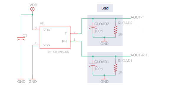
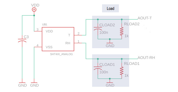
The sensor circuit was designed using a Sensiron SHT4X series analog sensor. This sensor was chosen for its ability to function and survive in high-temperature environments. The standard circuit schematic, which was outlined by the manufacturer’s guidelines, is shown in Fig. 2 (“Datasheet -SHT4x 4 Th Gen. Relative Humidity and Temperature Sensor Highlights,” n.d.).
The print file for the circuit was designed using AutoCAD and is shown in Fig. 3. The power and ground traces were designed to have a width of 1000 um, and the signal-carrying traces were designed with a width of 500 um.

III. Material and Process Optimization
A. Dielectric Substrate
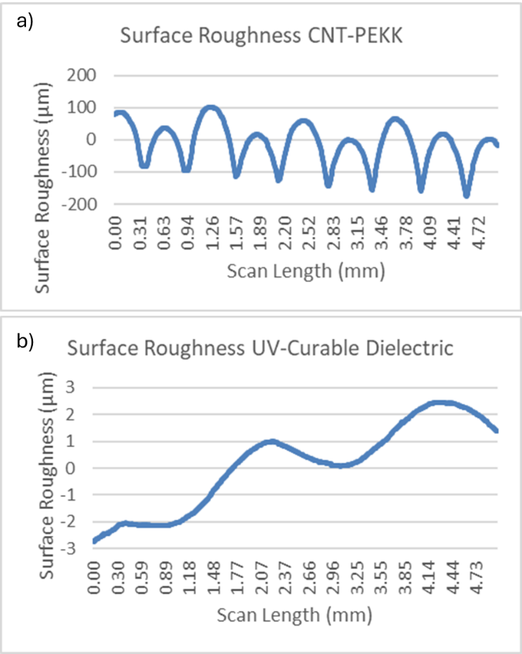
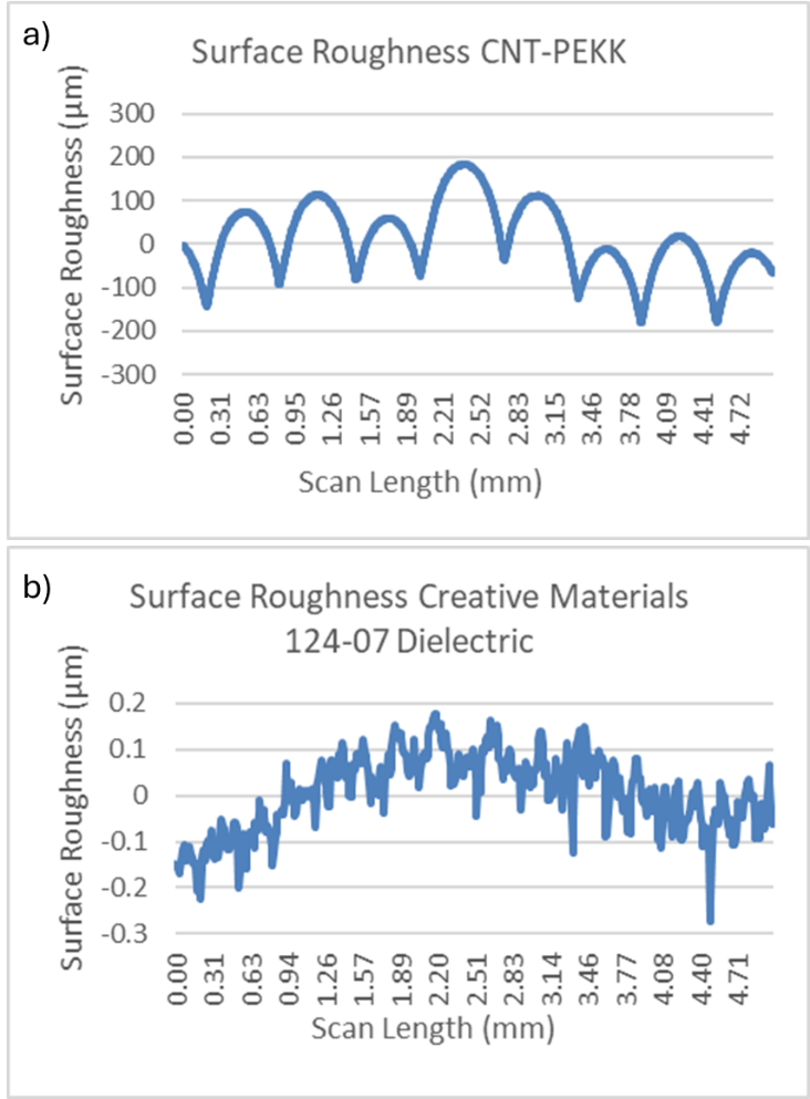
Due to the conductive nature of the CNT-PEKK, a dielectric insulating layer was necessary to shield the conductive traces. This dielectric layer also served as a planarizing coating to decrease the effects of the surface roughness that are inherent in FDM printing. Initially, the CNT-PEKK was planarized using a custom UV-curable dielectric because of its ability to wet to PEEK, which has similar wetting characteristics to PEKK, as demonstrated in prior work (Lamport et al. 2023; Maiti et al. 2024). This UV curable ink was deposited onto the CNT-PEKK using a Nordson Pro4. In this work, to streamline manufacturing, and to meet the criteria for high-temperature applications, a commercially available, high-temperature laminating adhesive from Creative Materials (CM124-07) was used. To ensure proper coating of the CNT-PEKK, surface roughness measurements were taken before and after the deposition of the dielectric. The surface roughness of the dielectrics was measured using a Bruker ContourGT Optical profilometer, and the surface roughness measurements of the CNT-PEKK were performed using a KLA-Tencor stylus profilometer, due to the optical absorption of the CNT-PEKK. Fig. 4 shows the average surface roughness before and after planarization using the UV-curable dielectric, and Fig. 5 shows the average surface roughness before and after planarization using the commercially available printed dielectric.
_cnt-pekk_prior_to_planarization__b)_cnt-pekk_post-planarization_with_uv-curable_dielect.png)
_cnt-pekk_prior_to_planarization__b)_cnt-pekk_post-planarization_with_creative_materials.png)
B. Silver Ink
To print the conducting traces of the sensor, a commercially available silver ink and conductive epoxy hybrid ink for high-temperature applications, from Creative Materials (CM126-40) was used. Since this ink was used for both the traces and the conductive epoxy for the component attachment, fewer materials were used, which increased material compatibility. During extrusion, the force inside the flow path caused cold fusion of the silver nanoparticles in the tip, leading to inconsistent printing and clogging. Hence, careful optimization was required to determine which parameters resulted in the most consistent printing.

Regarding the uniformity of the printed silver traces, the infill angle was found to be a significant factor. To determine this, the analog silver traces were printed using three different infill angle orientations: 0⁰, 45⁰, and 90⁰. The linewidth was measured at least five times in different locations, which are labeled in Fig. 6. From these measurements, the standard deviation was calculated for each group, as shown in Fig. 7.

From the above figure, the samples printed with a 90⁰ infill angle had consistently lower standard deviation values than samples printed with either 0⁰ or 45⁰ infill angles. Hence, for the remaining of the prints, the 90⁰ infill angle was used.
Another factor that affected the quality of the printed silver was the piston used in the dispensing syringe. The piston is designed to create an even pressure differential and fluid flow inside of the piston when pneumatically activated. In most ink applications, the white piston from Nordson is sufficient to use. In high-viscosity applications, however, the piston does not provide the right pressure differential to sufficiently move the ink. The piston moves up and down in the syringe—a phenomenon known as “piston bouncing.” The force that the piston exerts on the ink when it is bounced leads to cold fusion of the nanoparticles in the silver ink. This leads to an increase in the occurrence of clogging in the tip, which slows manufacturing time and can reduce the overall quality of the printed traces. To combat this, a flexible clear piston from Nordson was used inside of the dispensing syringe. The flexibility of the piston allows for dynamic change in the pressure differential to allow the ink to flow more smoothly and to prevent piston bouncing from occurring. Once the conducting traces were printed, the conductive epoxy (CM 126-40) was printed to connect the SMT component leads to the silver traces, and then the nonconductive epoxy (CM 124-07) was deposited where the center of the chips would be placed to increase the mechanical robustness of the printed sensor. Both epoxies were printed using a Tabletop nScrypt SmartPump. Once the epoxies were printed, the components were placed using an nScrypt 3Dn-300 Pick-n-Place head. Fig. 8 shows a finished printed circuit.

IV. Results
A. Electrical Testing
Once the sensor printing was completed, electrical testing was performed to assess the performance of the circuit. The circuit was powered to 5V and the output voltage at pin #1 (Relative Humidity (RH)) and pin #2 (Temperature) were measured. The measured voltage at pin #1 was inserted into Equation 1 to calculate RH, and the measured voltage at pin #2 was inserted into Equation 3 to calculate temperature in degrees Fahrenheit.
RH=(−12.5+125∗VRHVDD)%RH=−100.8+1000.8(VRHVDD)%RH
T=(−66.875+218.755∗VTVDD)(∘C=−45−17.50.8+1750.8(VTVDD)(∘C
T=(−88.875+393.75∗VTVDD)(∘F=−49−31.50.8+3150.8(VTVDD)(∘F
The relationships between the output and source voltage ratio compared to RH and temperature are shown in Fig. 9 (“Datasheet -SHT4x 4 Th Gen. Relative Humidity and Temperature Sensor Highlights,” n.d.).
_and_tempera.png)
These measurements were taken on three different days to monitor the variability of the measured values. The voltage output measurements are shown in Table 1, and the calculated RH and temperature values are shown in Table 2. The values obtained from the sensor were compared to RH and temperature values obtained from a Govee H5074 Bluetooth RH and temperature sensor.
To test the performance over multiple temperature and humidity ranges, the analog circuits were subjected to temperature cycling over multiple relative humidities. This was done in an ESPEC environmental chamber. The results are shown in Fig. 10.

The temperature and RH cycling of the sensor circuit through varying RH levels shows good agreement of the control measurements in the chamber, which is measured by a thermocouple. The plateau seen in the temperature graph can be attributed to the temperature of the chamber exceeding that of the operating temperature of the sensor, which is 125°C. Differences in the measurements of temperature can be attributed to two main causes: (1) increased resistance on the printed traces providing less current to the sensor, and (2) lack of calibration for the resistance when measuring the voltages required to extract the temperature and RH data.
B. Mechanical Testing
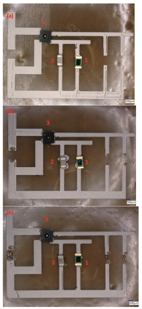
To quantify the strength of the bond of the epoxies between the SMT components and the silver traces, die-shear testing was performed. It was hypothesized that the SMT components would be most robust when nonconductive and conductive epoxies were used to bond the chips to the silver traces and the substrate to increase the mechanical robustness and the quality of the electrical connection, respectively. The non-conductive epoxy is used to bond the chips to the substrate, and its purpose is to add mechanical robustness to the mounting of the chips. The conductive epoxy is mounted between the terminals of the SMT components and the silver traces and provides the electrical connection between them. Three samples were prepared with three chips, each used in the analog sensing circuit, to optimize the surface mount process of the components. The details of the sample fabrication area are shown in Fig. 11 (a)-(c).
_chips_1_(1k_resistor)__2_(100_.png)
The die shear testing was performed on each chip on each sample using a Chatillon KMP model 1750. A load force was applied laterally to each chip until it was removed. The load force at which the chip was dislodged was then used to calculate the maximum lateral stress of each chip. The results of the die shear testing are shown in Figure 12, for the three samples shown in Fig. 11 (a)-(c), respectively (Pan et al. 2006).
__c)_results_of_the_mechanical_shear_testing_in_max_load_force_(n)_and_max_stress_(mpa.png)
The cured silver traces and the conducting epoxy led to better mechanical results. The maximum stress values of traditional solder materials SAC305 and SnPb for similarly sized SMT packages is 65 MPa and 75 MPa, respectively, and the maximum load force is 30 N and 35 N, respectively. The maximum stress and maximum load force is much greater in the solder materials than the results obtained during the die shear testing due to the epoxy chemistry being significantly more brittle than the chemical makeup of the traditional solder materials. To increase the robustness of the sensor, the components will be encapsulated for future work.
C. Statistical Analysis
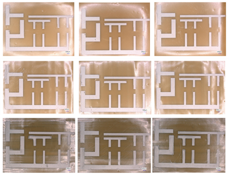
To ensure print uniformity of the silver lines over continuous printing intervals, a gauge repeatability and reliability (Gage R&R) analysis was performed (Hessing, Pv, and Naomi 2024). The two methods of this analysis include the Mean-Range method and the Analysis of Variance (ANOVA) method, both of which were utilized to assess the print uniformity. Three samples were printed over three days, each with three prints per sample. These samples are shown in Fig. 13.
__2_(middle_row)__and_3_(bottom_row)_for_gage_r_r_studies.png)
The results from both the Mean-Range method and the ANOVA method for gage R&R are shown in Table 3.
According to the specification of this analysis, the acceptable range is <10% and <1% for the Mean-Range Method and ANOVA method, respectively. The results for the measured linewidths of the 1000 and 500 um lines and the thicknesses were all within these acceptable ranges (Hessing, Pv, and Naomi 2024).
V. Conclusion
This work has demonstrated not only the successful completion of a printed temperature and humidity sensor for use at high temperatures, but it has also demonstrated optimizations in both print processes and material handling to increase the efficiency and quality of the manufactured sensors. These optimizations are vital to allowing the widespread adoption of AM as an independent manufacturing technique. With the growing need for nontraditional circuit designs, these optimizations are vital for future innovations in a variety of technologies.
Acknowledgment
This material is based upon work supported by the ACC-APG Adelphi Contracting Division Army Research Laboratory under Contract No. W911QX-22-C-0015. All material, except scientific articles or papers published in scientific journals, must, in addition to any notices or disclaimers by the Contractor, also contain the following disclaimer: Any opinions, findings and conclusions or recommendations expressed in this material are those of the author(s) and do not necessarily reflect the views of the ACC-APG Adelphi Contracting Division Army Research Laboratory