


1. Introduction
As technology advances, wire bonding faces ongoing challenges in meeting the demands for miniaturization, high-density packaging, and improved electrical performance (Zhou et al. 2023). Wire bonding is found to be problematic at advanced nodes and in complex chips. As the number and density of bond pads increase, there is limited space to ensure wires don’t touch or cause interference. This is where advanced packaging technologies, such as thermo-compression (TCP) bonding and flip-chip packaging technologies, may have a role. These techniques utilize solder or Cu bumps to create direct connections between the chip and the substrate, eliminating the need for long wire interconnects. As a result, they offer a more compact, efficient, and high-performance solution for modern semiconductor devices, particularly those in high-frequency applications where wires create inductance leading to electrical parameter issues. However, the cost and process complexity of TCP and flip-chip technologies have been major hindrances over wire bonding. Wire bonding offers flexibility to match different dies to standard leadframe and substrate designs, and they often are more cost effective than flip-chip alternatives (Marks, Hassan, and Cheong 2015). With wire bonds, the same die can be assembled into different package form factors, giving end users flexibility to fit the package that best suits the system or assembly process technology’s needs. Therefore, wire bonding remains a widely adopted and well-established technology due to its versatility, reliability, and cost-effectiveness.
A widely reported issue faced by wire bonding on Al bond pad is the impediment of intermetallic compound (IMC) formation between the wire material and the pad metallization caused by the presence of aluminum fluoride crystals on discolored pad surfaces (Ernst et al. 1994; Alberici et al. 2003; Younan, Xiang, and Xiaomin 2014; Pani et al. 2018; Senthilkumar, Shee, and Rao 2022; Gross et al. 2007; Daniel et al. 1990). The aluminum fluoride crystals act as an interdiffusion barrier, causing a lack of IMC formation and a mechanically weak interface between the wire and the pad. Weak wire bonds may lead to non-stick-on-pad (NSOP) during the wire bonding process, lifted wires in the semiconductor package, and high ohmic resistance which pose serious electrical and reliability problems in the semiconductor device.
Residual fluorine on the Al bond pad has been attributed to the reactive plasma etching of passivation dielectric layers (e.g., polyimide, SiN, SiOx) above the bond pad (bond pad opening process) employing hydrofluorocarbon gases such as CHF3, CF4, SF6, and NF3. Previous studies on the aluminum fluoride crystals that form on the bond pad surface due to residual fluorine reactions indicate that they can have various morphologies and chemical states, primarily aluminium fluoride (AlFx), aluminum oxyfluoride (AlxOyFz), and their hydrates, depending on fluorine level and environmental condition (Ernst et al. 1994; Alberici et al. 2003; Younan, Xiang, and Xiaomin 2014). Various bond pad cleaning processes to significantly remove the fluorine residues have been proposed e.g., biased Ar sputtering (Alberici et al. 2003), optimization of the dielectric plasma etching process (Pani et al. 2018), and a combination of plasma and wet resist etching (Pani et al. 2018; Senthilkumar, Shee, and Rao 2022). Although similar fluorine removal processes have been evaluated in our wafer fabrication flow, we observe that the fluorine concentration on the bond pad increases with longer storage time, resulting in aluminum fluoride crystal growth. Fig. 1 shows the increasing trend of fluorine concentration on the Al bond pad after the dielectric etching and pad cleaning processes as measured by Auger electron spectroscopy (AES). Even though the initial fluorine concentration immediately after pad cleaning was below 5 at.%, the concentration increased to more than three times the initial value with storage times close to 200 days. The mechanism of increase of fluorine concentration on Al bond pads, the mechanism of aluminum fluoride crystal formation, and the prevention methods are not well understood.

This work focuses on investigating the mechanism of fluorine concentration increase on the Al bond pad with storage time, the mechanism of aluminum fluoride crystal formation, and the prevention methods. The effects of various wafer storage methods on the fluorine concentration were studied systematically. Based on the results from this study, the best storage methods were recommended to effectively prevent the occurrence of pad discoloration.
2. Experimental procedure and results
2.1. Analyses of discolored Al bond pads
Al bond pads affected by aluminum fluoride crystal growth will typically appear to be discolored when inspected under an optical microscope. The following sub-sections cover the analyses performed on the discolored pads to understand its surface morphology and chemical composition.
2.1.1. Scanning electron microscopy (SEM)
The morphology of an affected Al bond pad surface was studied at high magnification using a Hitachi S4800 field-emission SEM. Fig. 2 shows a SEM image of the surface of a typical Al bond pad containing aluminum fluoride crystals of varying densities. Regions of rougher surface morphology have a higher density of crystals with a crystal size range of approximately 0.3-0.5 µm, while regions of smoother surface morphology have a lower density of crystals with a crystal size range of less than 0.1 µm. The crystal structure appears to be predominantly hexagonal.

2.1.2. Transmission electron microscopy (TEM)
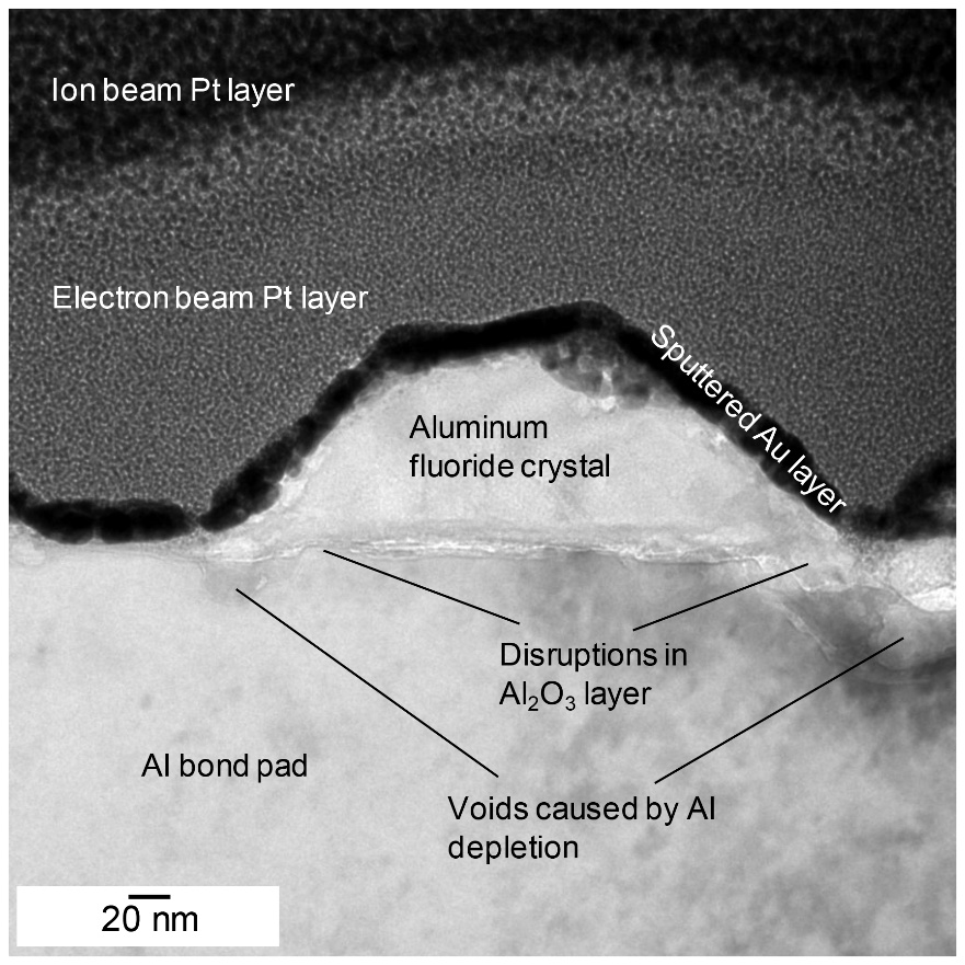
A TEM lamella of the cross section of an affected Al bond pad was prepared using SII NanoTechnology Xvision 200 Focused Ion Beam (FIB). The ion milling conditions were: 30 kV Ga+ ion source accelerating voltage; 250 pA beam current. Protective coatings consisting of sputtered Au, and electron beam/ion beam-assisted chemical vapor deposition Pt were deposited on the sample surface prior to ion milling. The lamella was mounted to a Mo TEM grid. The lamella thickness is approximately 100 nm after final ion polishing. A FEI Tecnai G2 F20 X-Twin 200 kV field-emission TEM was used for sample analysis. Scanning transmission electron microscopy (STEM) mode was used for brightfield imaging and energy dispersive spectroscopy (EDS) analysis.
Fig. 3 is the TEM bright field image of an Al pad surface region which is flat and without any aluminum fluoride crystals. A native Al2O3 layer of approximately 7-8 nm thickness can be seen. Fig. 4 is the TEM bright field image of an Al pad surface region containing aluminum fluoride crystals. Disruptions in the native Al2O3 layer underneath the crystal were observed, forming paths for Al supply for the aluminum fluoride crystal formation and growth. Voids in the Al have been formed below the crystal due to the depletion of Al. Fig. 5 shows the EDS line scan across an aluminum fluoride crystal at the Al pad surface indicating the presence of Al, F, O and low level of C. The thickness of the aluminum fluoride crystal is approximately 80-90 nm. It is to be noted that the high C content in the FIB protective coating layers is attributed to organic residues from the electron beam/ion beam-induced decomposition of the organometallic gas precursors during the FIB deposition of the Pt protective layers.


2.1.3. X-Ray Photoelectron Spectroscopy (XPS)
XPS analysis was performed with a Thermo Scientific ESCALAB Xi+ spectrometer to determine the elements present on the Al pad surface and their chemical states. A standard Al Kα monochromatic X-ray source was used. The typical measuring conditions were as follows: X-ray power, 15 kV, and 20 mA; X-ray spot size, 30 µm; electron pass energy through the analyzer, 20 eV; spectrometer base pressure, less than 10-9 mbar. Data was collected using a hemispherical analyzer fitted with a six-channeltron detector. Specimen charging was compensated with the electron flood gun using the Cls binding energy for aromatic/aliphatic C-C/C-H at 284.5 eV as the reference. The Al pad was analyzed with an electron take-off angle of 90°. The experimental uncertainty of binding energy was ±0.1 eV, while the relative error for quantitative analysis is ±3-10%.
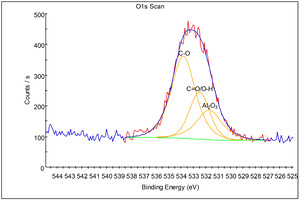
XPS analysis was performed on an affected Al bond pad with an analysis area of approximately 30 µm diameter. The deconvoluted O1s peaks (Fig. 6) at 531.7 eV, 532.5 eV and 533.8 eV are attributed to native Al2O3, C=O/O-H and C-O, respectively (“NIST X-Ray Photoelectron Spectroscopy Database” 2023; Olefjord, Mathieu, and Marcus 1990; Marcus, Hinnen, and Olefjord 1993). The presence of some organic impurities, as was also detected by EDS, is most likely due to minor organic residues from the use of organic gas precursors in the deposition and etching processes. The F1s peak (Fig. 7) at 686.0 eV is attributed to AlF3 (“NIST X-Ray Photoelectron Spectroscopy Database” 2023; Strohmeier 1989). The deconvoluted Al2p peaks (Fig. 8) at 73.1 eV, 75.4 eV and 76.7 eV, are attributed to Al metal, native Al2O3, and AlF3, respectively (“NIST X-Ray Photoelectron Spectroscopy Database” 2023; Olefjord, Mathieu, and Marcus 1990; Marcus, Hinnen, and Olefjord 1993; Strohmeier 1989; Chang, Anderegg, and Thiel 1996).


2.2. Evaluation of wafer storage methods.
Based on wafer monitoring results, the fluorine concentration on the Al bond pad increases with longer storage time as shown in Fig. 1. Standard polypropylene wafer boxes with a removable wafer carrier (Fig. 9) are used and the boxes are placed on open racks in a cleanroom environment with average temperature and humidity of 22ºC and 45% RH, respectively. The wafer carrier has 25 vertical slots for 200 mm wafers. The seam between the wafer box top cover and base is not airtight and allows air or gas to flow through.
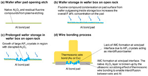
It is hypothesized that the increase in fluorine concentration on the Al bond pad is potentially due to outgassing of fluorine compounds which have been adsorbed on the surface of the wafer during plasma etching and subsequent condensation of these compounds on the pad surface. In order to investigate this hypothesis and the influence of wafer storage methods on fluorine concentration on the Al bond pad, the experimental flow shown in Fig. 10 was carried out. Six different methods of wafer storage were evaluated and compared. In this experiment, two types of 200 mm Si wafers were utilized: finished CMOS technology wafers with Al bond pad metallization and polyimide passivation, and test wafers with blanket Al metallization for XPS analysis. The Al metallization layer on the test wafers is 800 nm thick and was deposited by physical vapor deposition (PVD), representative of the Al metallization layer in the CMOS technology wafers.
The experiment is segmented into three groups. The first experiment group is based on the standard wafer box described earlier in Fig. 9, which is typically used for storage of in-process wafers at the wafer fabrication site. Within the wafer box group, four storage methods were evaluated: 1) wafer box placed on open rack; 2) wafer box placed in N2 cabinet; 3) wafer carrier placed in N2 cabinet (without outer box); 4) wafer box sealed in moisture-barrier bag (MBB) and placed on open rack. The wafer carriers in the boxes were filled with twenty-four wafers with one test wafer placed in the middle slot. The humidity level inside the N2 cabinet is controlled at 5-10% RH, verified using a Rotronic Hygrolog HL-NT2 portable humidity data logger. For the MBB packing, a desiccant pack is included inside the bag before vacuum sealing. The humidity level inside the MBB packing with desiccant was verified using a humidity indicator card to be about 10% RH. The second experiment group is based on the standard polypropylene wafer canister as shown in Fig. 11. The seam between the top cover and the base of the wafer canister is not airtight and allows air or gas to flow through. The current industry practice is to ship finished wafers in wafer canisters sealed in MBB with desiccant to the packaging assembly site. At the packaging assembly site, the MBB will be opened for incoming wafer inspection. After wafer inspection, the wafer canisters will then be stored in N2 cabinets without MBB, pending the assembly process of the wafers. Within the wafer canister group, two storage methods were evaluated: 1) wafer canister sealed in MBB and placed on open rack; 2) wafer canister placed in N2 cabinet. The wafer canisters were filled with twenty-four wafers and a test wafer is placed in the middle of the wafer stack. Wafers were separated by Tyvek® interleaf films (“DuPontTM Tyvek® Industrial Packaging Brochure” 2021) and a polyethylene foam pad is placed at the top and bottom of the wafer stack. The third experiment group are the controls for the wafer box and wafer canister: 1) wafer box placed on open rack; 2) wafer canister placed on open rack. For the wafer box control, a test wafer was placed in the middle slot of the wafer carrier and the rest of the slots were empty. For the wafer canister control, only one test wafer was placed inside the box with Tyvek® interleaf films and polyethylene foam pads below and above the test wafer. All storage methods underwent a storage time of six weeks, after which the test wafers were removed for XPS analysis. XPS analysis was performed on the test wafers with an analysis area of approximately 50 µm diameter at the center location of the wafer. This is reasonable as the pad discoloration locations in affected wafers are random in nature. The fluorine concentrations were measured by XPS instead of Auger as the values obtained by Auger may be relatively lower than XPS because of electron beam-induced degradation to the fluorine compounds (Lichtman and Kirst 1966). The results of the XPS analyses of the wafer box group and the wafer canister group are tabulated in Table 1 and Table 2, respectively. The control values have been included in both tables. Fluorine was not detectable in both control samples, indicating that the cleanroom atmosphere and materials in the wafer box and wafer canister did not cause any fluorine contamination on the test wafers.


3. Discussion
The hexagonal crystal structure of aluminum fluoride observed on the discolored Al bond pads have similarly been observed by other workers but the crystal structure and chemical composition are not well understood (Younan, Xiang, and Xiaomin 2014; Pani et al. 2018). Currently, there is a limited amount of crystallographic data for aluminum fluoride compounds. The thermodynamically stable phase of the aluminum fluorides, α-AlF3, has a rhombohedral crystal structure at room temperature (Gross et al. 2007; Daniel et al. 1990). The β-AlF3 phase has an orthorhombic structure, while the highly disordered high surface area phase, HS-AlF3, is amorphous (Gross et al. 2007; Daniel et al. 1990). The stable hydrated form of aluminum fluoride, AlF3.3H2O, has a tetragonal crystal structure (Nielsen and Altintas 1984; Bayat, Taeb, and Rastegar 2005). Vasiliev et al (Vasiliev, Melnikova, and Isaenko 2009). reported that stoichiometric aluminum oxyfluoride, AlOF, has an orthorhombic crystal structure. Kutoglu (Kutoglu 1992) reported that non-stoichiometric aluminum oxyfluoride, Al1-xO1-3xF1+3x (x = 0.0886), has a tetragonal crystal structure. While there is no direct correlation between these reported crystal structures of various aluminum fluoride compounds and the observed hexagonal crystal structure on the Al bond pad, there is a likelihood of phase transformation of rhombohedral α-AlF3 to hexagonal form due to stacking faults occurring periodically during crystal growth or due to creation and movement of Shockley partials (Agrawal 1979). XPS analysis has ascertained that the chemical composition of the aluminum fluoride crystals on the Al bond pad is AlF3. Further work is planned to confirm the AlF3 crystal structure by TEM diffraction analysis.
In the standard wafer box experiment group, the lowest fluorine concentrations on the test wafer were obtained by placing the wafer carrier inside a N2 cabinet (1.7 at.%), and by placing the wafer box inside a N2 cabinet (3.9 at.%), compared to placing the wafer box on an open rack (10.0 at.%). However, the wafer box sealed in MBB with desiccant showed a higher fluorine concentration (8.6 at.%). In the standard wafer canister experiment group, significantly lower fluorine concentrations on the test wafer were obtained by sealing the wafer canister in MBB with desiccant (1.5 at.%), and by placing the wafer canister in a N2 cabinet (1.1 at.%). The results of the storage experiment confirm that an outgassing-condensation mechanism is responsible for the increase in fluorine concentration on the Al bond pads which will subsequently lead to aluminum fluoride crystal growth (Fig. 12). Fluorine compounds can be adsorbed on the surface of the polyimide passivation by physisorption or chemisorption during the plasma etching process. These fluorine compounds will subsequently outgas from the polyimide surface and condense on the Al bond pad surface of wafers inside the storage box.

From the results of the wafer storage experiment, it can be inferred that three storage-related factors play an important role in the outgassing of fluorine compounds from the polyimide surface and condensation of fluorine compounds on the Al bond pads. The first factor is the humidity level in the wafer storage. The humidity level in a wafer box placed on an open rack will equilibrate with the cleanroom humidity of 45% RH. The corresponding fluorine concentration on the test wafer is 10.0 at.% after six weeks of storage time. In comparison, the humidity level in a wafer box sealed in MBB with desiccant is about 10% RH and the corresponding fluorine concentration is 8.6 at.% after the same storage duration. The approximately 35% RH reduction in the humidity level inside the wafer box sealed in MBB with desiccant appears to reduce the fluorine concentration by about 1.4 at.%. A plausible explanation is that the fluorine compound molecules adsorbed on the polyimide surface may be extracted by water molecules through dipole-dipole attraction forces and this enhances the outgassing process. In a study of the effect of relative humidity on the outgassing of volatile organic compounds from paper and board, Wolf et al (Wolf, Hoyer, and Simat 2023). found that the outgassing of polar substances are more influenced by increasing humidity. The second factor is the displacement of fluorine outgassing species by N2 in the wafer storage. Inside the N2 cabinet, the diffusion of N2 molecules into a wafer box will gradually displace and flush out the fluorine compound molecules from the wafer box, eventually lowering the amount of fluorine compound condensation on the test wafer (3.9 at.%). In the case of a wafer carrier placed inside the N2 cabinet, the relatively higher flow rate of N2 molecules in between the wafers will rapidly flush away the fluorine compound molecules thereby limiting the amount of condensation on the test wafer (1.7 at.%). Storage of wafers (in wafer box or wafer carrier) in a N2 cabinet shows a much higher effectiveness in reducing fluorine compound condensation on the Al bond pads compared to wafer box sealed in MBB with desiccant where there is a reduction in humidity only, assuming comparable humidity levels in the three storage methods. The third factor is the restriction of outgassing from the polyimide surface by sandwiching an interleaf film between wafers. The Tyvek® interleaf film is porous and breathable (“DuPontTM Tyvek® Industrial Packaging Brochure” 2021). It physically traps or adsorbs the fluorine compound molecules on the polyimide surface to slow down the outgassing rate inside a wafer canister. For a wafer canister sealed in MBB with desiccant, the fluorine compound condensation (1.5 at.%) is slightly lower than that of a wafer carrier placed in a N2 cabinet (1.7 at.%). Storing wafers in a wafer canister inside a N2 cabinet produces the lowest amount of fluorine compound condensation (1.1 at.%) compared to all the other storage methods because of the possible combined effects from all three factors.
A comparison of various wafer technologies revealed that wafers with a polyimide surface area ratio of above 40% are more prone towards having Al bond pad discoloration related to fluorine. This indicates the dependency of the fluorine compounds adsorption and outgassing on the polyimide surface area. Further work is needed to understand the rate and depth of adsorption of fluorine compounds in the polyimide passivation surface during plasma etching and the rate of outgassing of fluorine compounds during storage. This understanding will be helpful in the optimization of the polyimide bulk and surface properties and the plasma etching parameters to minimize adsorption and outgassing.
Based on production monitoring data, storing wafers in wafer boxes placed on open racks may result in Al bond pad discoloration after a few weeks. So far, inspection of in-process wafers stored in wafer boxes placed in N2 cabinets did not show any Al bond pad discoloration up to nine months of storage. Monitoring of wafers stored beyond nine months is currently ongoing. Although storing wafers in wafer carriers placed in N2 cabinets results in a relatively lower increase in fluorine concentration, owing to the risk of handling damage and particulate contamination on the exposed areas of wafers in a wafer carrier, it was not recommended to use this storage method in production. So far, inspection of finished wafers shipped to the packaging assembly site in wafer canisters sealed in MBB with desiccant and inspection of finished wafers in wafer canisters stored in N2 cabinets did not show any Al bond pad discoloration up to twelve months of storage. The waiting time for wafers received at the packaging assembly site before being loaded into the assembly process is typically less than a few weeks. Therefore, the two wafer canister storage methods provide adequate protection for wafers from Al bond pad discoloration at the assembly site.
4. Conclusions
Through this work, the mechanism of increase of fluorine concentration on Al bond pads, the mechanism of aluminum fluoride crystal formation, and the prevention methods are better understood. Al bond pad discoloration has been mainly caused by the growth of aluminum fluoride crystals through an increase in the fluorine concentration on the pad surface attributed to the outgassing-condensation mechanism occurring inside the wafer storage. TEM analysis revealed that disruptions in the native Al2O3 layer underneath the aluminum fluoride crystal form paths for Al supply for the crystal formation and growth, forming depletion voids in the Al surface. The chemical composition of the aluminum fluoride crystals has been ascertained by XPS to be AlF3. A detailed study of the effects of wafer storage methods on fluorine concentration on Al metallization of test wafers revealed three storage-related factors that influence the outgassing of fluorine compounds from the wafer polyimide passivation and condensation of fluorine compounds on the Al bond pads: humidity level, displacement of fluorine outgassing species by N2, and restriction of outgassing by wafer interleaf film. Careful consideration of these key factors will help in deciding on appropriate wafer storage methods to prevent Al pad discoloration.
At the wafer fabrication site, storage of in-process wafers (in wafer box or wafer carrier) in a N2 cabinet shows a much higher effectiveness in reducing the fluorine compound condensation on the Al bond pads. Owing to the risk of handling damage and particulate contamination of wafers stored in wafer carriers, storage of wafers in wafer box placed in N2 cabinet is preferred. At the packaging assembly site, the wafer canister storage methods (wafer canister sealed in MBB with desiccant, and wafer canister in N2 cabinet) provide adequate protection for finished wafers from Al bond pad discoloration. These wafer storage methods have effectively prevented the occurrence of fluorine-induced Al bond pad discoloration over prolonged wafer storage times in both the wafer fabrication and packaging assembly sites.
Acknowledgements
The author would like to thank Lim Joon Hoong, Nur Suhaili Abd Aziz, and Lingeswarran Muniandy for their support.