

I. Introduction
The electronics industry is undergoing rapid transformation, driven by the increasing demands of artificial intelligence (AI), high-performance computing (HPC), and advanced computing applications such as GPUs, AI accelerators, and cloud computing. These advancements require sophisticated semiconductor technologies that can support complex computations and massive data processing. Integrated Circuit (IC) substrates, which form the critical link between microchips and printed circuit boards (PCBs), play a pivotal role in meeting these demands. With the IC substrate market projected to reach $34 billion by 2028, the industry is poised to capitalize on the high-density connectivity and performance demanded by modern electronic devices (Wang et al. 2017).
To meet these needs, advanced packaging technologies such as 2.5D interposers, embedded bridges, and High-Density Interconnect (HDI) methods have emerged as key enablers. Among these, modified Semi-Additive Processing (mSAP) has become crucial for fabricating finer features such as high-density redistribution layers (RDL), stacked vias, and plated fine traces. The transition from traditional subtractive processes to mSAP supports the direct attachment of chips to organic IC substrates and enables higher signal routing densities critical for AI and HPC applications. Additionally, mSAP enhances reliability by creating precise, rectangular fine lines that optimize circuit density, achieve impedance control, and minimize signal loss.
However, the increasing complexity and miniaturization of IC substrates introduce several technical challenges. Larger Flip Chip Ball Grid Array (FCBGA) units and advanced packaging formats require intricate designs with precise line spacing, uniform line-and-space (L/S) dimensions, and reliable via connectivity. Achieving flat via tops, consistent plating uniformity, and effective thermal management becomes essential to ensure performance and reliability, particularly as line/space dimensions shrink to ten μm. These challenges push the limits of lithography, etching, and plating technologies.
mSAP is critical for producing advanced IC substrates and Printed Circuit Boards (PCBs). However, the process is not without its challenges. One key issue is achieving consistent plating uniformity across fine lines and vias. Traditional processes often lead to non-uniform copper deposits, resulting in defects such as voids, seam voids, and uneven thicknesses (Lee and Chen 2018).
Another challenge is the reliance on specific electroplating tools and configurations. Many existing copper plating processes are tailored to equipment, requiring significant capital investment to implement new formulations or adapt to different systems. This tool dependency limits flexibility and scalability in manufacturing operations.
In addition, during the flash etching step of mSAP, issues such as V-pits, can arise. These defects may compromise copper interconnect reliability. They are often addressed using additional baking steps. However, such steps are energy-intensive, increase production costs, and reduce throughput, making them less favorable for high-volume manufacturing (Moffat, Wheeler, and Josell 2004).
This study introduces an optimized copper electroplating process that addresses these challenges holistically. By utilizing a novel additive system which yields pure Cu deposits and promotes a bottom-up filling mechanism, the process ensures a uniform and defect-free copper deposition, effectively eliminating voids and seam voids. Its tool-agnostic design makes it compatible with a wide range of electroplating systems, such as Vertical Continuous Plating (VCP) and High-Speed Plating (HSP), reducing dependency on specific equipment.
The proposed process demonstrates excellent via filling capabilities, high fine line resolution, and consistent plating uniformity. Analytical results show superior physical properties, including high tensile strength and elongation, exceeding IPC class III requirements. By eliminating the need for baking while delivering uniform, reliable copper deposits, this process provides a scalable, efficient solution that meets the demands of AI and HPC applications.
II. Experiments
Acid Copper Electroplating
Electroplating has become a standard method for filling small features in PCBs, due to its cost-effective nature and practicality. This process involves using high concentrations of copper sulfate (up to 200-250 g/L) and lower concentrations of sulfuric acid (around 50 g/L) to promote rapid feature filling. The filling of these vias, which vary in size and shape, is controlled by organic additives designed to tailor the plating rate and achieve the desired physical properties of the copper deposit. Additives such as wetters, brighteners, and levelers play a critical role in controlling the quality of copper electroplating by influencing feature dimensions, yield, surface copper thickness, and overall distribution uniformity. Wetters and levelers both function as suppressors but interact differently with brighteners. Type I suppressors (wetters/carriers), typically high molecular weight polyoxyalkyl compounds shown in green in Figure 1, adsorb broadly across the cathode surface to reduce the plating rate and promote uniform metal distribution; however, they can be deactivated by brighteners. Type II suppressors (levelers), shown in red, are not deactivated and instead adsorb selectively at high current density sites—such as via edges—where they limit localized deposition. This prevents overplating and avoids premature closure, which can result in voids.
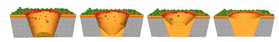
In Figure 1, the brightener, depicted in yellow, are small sulfur-containing molecules that enhance the plating rate by lowering the activation energy for copper deposition and refining grain structure. Due to their small size and high mobility, brighteners diffuse rapidly into microvias. As plating progresses and the via geometry changes, the concentration of brightener increases within the via, accelerating bottom-up deposition. This phenomenon is known as the Curvature-Enhanced-Accelerator Coverage (CEAC) mechanism, where the geometry-driven accumulation of brightener promotes rapid copper growth at the via base (Zhang et al. 2015). Once the deposit levels with the surface and the plating rate inside and outside the via equalizes, the bottom-up fill completes, resulting in a defect-free, uniform copper layer.
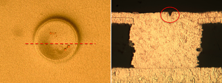
V-Pit
Wet chemical etching, flash etching, or chemical copper (Cu) reduction is a common practice in multilayer PCB fabrication. However, one significant issue during the Cu reduction step is uneven etching, which can result in defects such as V-pitting or pinhole formation (Moffat, Wheeler, and Josell 2004). These defects are characterized by small pits with diameters and depths typically ranging from 5–10 μm, as shown in Figure 2. Such pits compromise the mechanical and electrical reliability of copper interconnects, especially as line/space dimensions shrink below 10 μm.

To mitigate these defects, manufacturers often bake plated panels at 100–200°C for 1–3 hours. While this baking step can reduce pitting, it is energy-intensive and slows down production, creating a bottleneck for high-volume manufacturing. The additional energy consumption and reduced throughput make this approach less viable for cost-effective, scalable production.
As a result, the industry has a strong need for innovative copper plating solutions that produce deposits resistant to uneven etching and pitting, without requiring energy-intensive baking steps. Such advancements would significantly enhance manufacturing efficiency and improve the reliability of advanced electronic devices.
Plating Equipment and Parameters
Typical plating conditions for this process are shown in Table 1.
The process shown here is tool-agnostic. Two types of tools were employed Vertical Continuous Plating (VCP) with side educators, and High-Speed Plating (HSP) tools were used to evaluate via fill and uniformity.
VCP plating tools are designed for high volume manufacturing. Offering reliable performance for panel-scale plating processes, these tools feature basic adaptive anode systems and ion-exchange membranes, suitable for larger feature sizes and simpler plating requirements. The use of insoluble anodes ensures easier maintenance and consistent operation, avoiding the challenges associated with traditional solid copper anodes. Educators are incorporated to enhance solution agitation, providing adequate metal distribution across panel surfaces.
The VCP process is straightforward, starting with a pre-plating soak in a 10% wt H2SO4 solution to prepare the surface. Parameters are adjusted to achieve acceptable via filling and uniformity, catering to less demanding plating needs. VCP tools provide a cost-effective and dependable solution for manufacturers focused on standard plating applications without requiring the advanced features of more advanced systems.
HSP tools have transitioned from wafer level to panel level plating. They offer advanced features for panel-scale electrochemical deposition (ECD), including single-panel process modules, multi-zone anodes, and ion-exchange membranes, enhancing precision for smaller feature sizes down to 10 μm. The tool used in this study was an ASMPT NEXX P500 which uses insoluble anodes, avoiding the need for large solid copper anodes and ensuring consistent dimensions over time, with a more efficient metal replenishment system for higher deposition volumes. Post-plating uniformity was evaluated using a Keyence VK-X1000 profilometer, focusing on fine lines, pads, and filled vias across multiple dies, and intentionally excluding vias from uniformity calculations to minimize the influence of bumps or dimples.
Results and Discussion
V-pits originate from localized chemical attacks during flash etching, often in areas where the copper deposit is structurally weak or compositionally non-uniform. Industry studies suggest that these vulnerable regions are tied to the presence of organic impurities, structural discontinuities, or residual stresses embedded during electroplating. During copper electrodeposition, especially with aged plating baths or poorly tuned additive systems, impurities from organic additives or breakdown byproducts can become entrapped in the growing copper layer. These contaminants tend to concentrate along grain boundaries or discontinuities, forming pathways that later function as corrosion channels during etching (Moffat, Wheeler, and Josell 2004; Ho 2018). If these impurity-rich zones are not adequately mitigated, they accelerate localized etching and give rise to pitting. In extreme cases, vertical etch channels may develop into well-defined V-pits that penetrate deep into the copper layer, compromising electrical and mechanical reliability.
A study by Ho et al. highlighted that the presence of impurities, such as carbon (C), chloride (Cl), and sulfur (S), into the Cu plating will decrease the etching resistance of the Cu grains. As such, nanochannels—formed along high-defect-density grain boundaries in as-deposited copper—were a critical contributor to pinhole formation. [7, 8] These channels serve as localized corrosion initiation sites, particularly before copper undergoes any degree of grain relaxation or self-annealing. Although heat treatments can help suppress such defects by allowing grain coarsening and diffusion of impurities, these steps are not practical in high-volume manufacturing due to added cost, process time, and energy consumption.
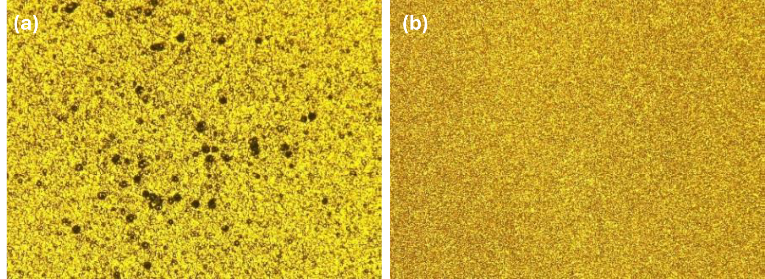
In contrast, our optimized copper plating process has been engineered to minimize impurities from the outset, removing the need for thermal annealing. Using a well-balanced additive system and controlled bath conditions, we ensure that the deposited copper is dense, uniform, and chemically pure. Secondary Ion Mass Spectrometry (SIMS) shown in Table 1 confirms low levels of residual carbon, sulfur, and oxygen across the plated layer—well below the critical threshold associated with pitting-prone microstructures. This high-purity copper shows superior resistance to localized etching, resulting in smoother surfaces and a marked reduction in V-pit formation. Figure 3 shows the V-pit resistance of prior technology compared to the new process during flash etching.
_prior_technology_after_9_m_flash_etch_showing_numerous_sites_of_v-pits._(b)_new_proce.png)
In summary, our plating system addresses V-pit formation through a proactive strategy—by delivering high-purity, defect-resistant copper deposits that resist corrosion from the start. This approach eliminates the need for post-deposition baking, improves manufacturing throughput, and ensures consistent reliability in fine-feature, high-density substrates used in AI, HPC, and next-generation electronic devices.
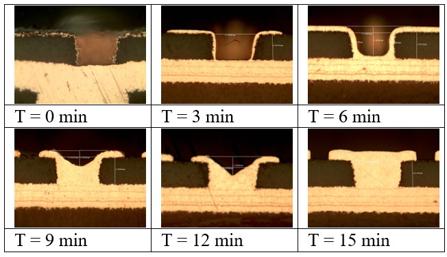
During a plating experiment, samples were taken every three minutes and subsequently cross-sectioned to observe the plating progress. Figure 4 shows how additives such as the wetter, brightener, and leveler work together to achieve a flawless bottom-up fill. At the 6-minute mark, it was observed that the bottom corners of the via began to plate more rapidly due to the concentration of the brightener in these areas. By the 9-minute mark, this led to a conical shape forming within the via. This process causes the brightener to further concentrate at the bottom, resulting in an accelerated bottom-up fill process that continues vigorously between 9 and 15 minutes. By carefully monitoring and controlling these parameters, a high-quality, defect-free copper deposit can be achieved, which is critical for the performance and reliability of the finished PCBs.

During the plating process, the shape of the via changes, causing the brightener to accumulate inside and accelerate the plating process. This phenomenon, called the Curvature-Enhanced-Accelerator Coverage (CEAC) mechanism (Zhang et al. 2015; Broekman et al. 2011), is essential to achieving the desired uniformity and quality in the electroplating process. The CEAC mechanism begins operating when the via’s geometry causes the brightener molecules to concentrate at the bottom, thereby accelerating the deposition rate in these areas. This continues until the via levels with the surface, at which point the bottom-up filling ceases, ensuring an even and defect-free copper layer.
Achieving a flat via top is also critical to overall build-up quality. Imperfections such as bumps or dimples introduce significant challenges in subsequent process steps. In stacked via structures, a non-flat via surface can scatter or deflect laser energy during laser drilling, leading to irregularly shaped or misaligned vias. These irregularities hinder the effectiveness of the bottom-up fill mechanism, making it difficult for additives to accumulate at the via base and initiate proper filling. As a result, defects such as incomplete fill, cavities, or seam voids can form as shown in Figure 5, reducing yield and compromising long-term reliability.

By enabling a faster deposition rate, high current density plating allows for shorter plating times, which is crucial for increasing throughput in the manufacturing of semi-conductor devices and IC substrates (Chen et al. 2015). This reduction in processing time not only minimizes energy consumption per unit of copper deposited but also lessens the wear and tear on plating equipment, thereby extending the lifespan of these costly tools. Shorter operation times also mean that these high-speed tools can handle more production cycles within the same timeframe, effectively reducing the cost of ownership by maximizing the utility of the equipment. Furthermore, the consistent and uniform copper deposits achieved through high Current Density(CD) plating reduce the incidence of defects such as inclusions and voids, enhancing yield and further diminishing the overall manufacturing costs. Thus, high current density electroplating is a critical technique for optimizing both the performance and cost-efficiency of modern electronic component fabrication. Figure 2 demonstrates that this process can fill vias without defects and with excellent uniformity across various CDs.
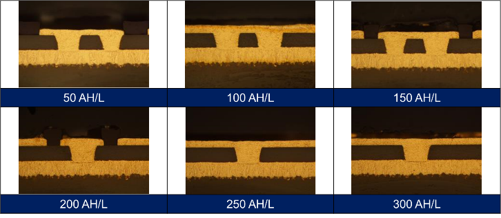
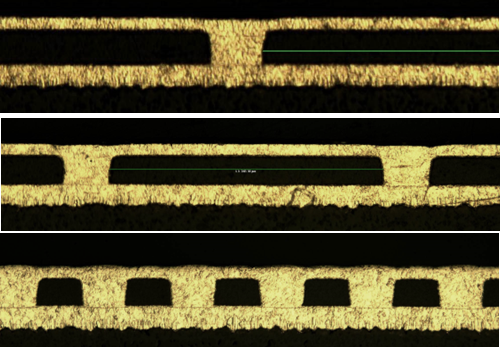
Following the initial evaluation, the bath was subjected to aging until it reached three hundred Ah/L. The volume of the bath was 8 L. The plating cycle for each plating was 15 ASF for 45 minutes, and the additive concentration was maintained as tabulated in Table 1. During the aging process, a test panel was plated at every 50 Ah/L, cross-sectioned, and evaluated under a microscope. The test board consisted of 60x35 µm vias and various L/S for fine lines. The plating cycle was adjusted to obtain around 15 µm on the surface. Throughout the entire aging process, consistent via filling was achieved, as shown in Figure 6.

Current IC substrate designs feature thousands of microvias that provide signal and power routing between layers. These vias may be isolated or densely packed to support the miniaturization requirements of advanced packages. Achieving uniform filling across varying via densities is a significant challenge, often leading to issues such as cavities, large dimples, or overfilling in certain areas. Figure 7 demonstrates the capability of the process under study to consistently fill microvias of differing densities without defects, ensuring high reliability and uniformity.

Copper (Cu) electrodeposit purity significantly impacts the performance of advanced IC substrates by influencing electrical resistivity and physical properties. Impurities such as sulfur and oxygen can increase electrical resistivity by disrupting the copper lattice and causing electron scattering, which degrades electrical conductivity. These impurities also affect physical characteristics by altering grain growth and epitaxial layer formations, potentially leading to smaller, less uniform grains that reduce ductility while increasing hardness.
Furthermore, during the etching processes, impurities can promote non-uniform etching and pitting, impacting the precision of circuit patterns and overall device reliability. Thus, maintaining high copper purity is essential for optimizing the functionality and longevity of IC substrates. Secondary Ion Mass Spectroscopy (SIMS) was employed to analyze the deposit for impurities, and the data is summarized in Table 2. According to the findings, the deposit is exceptionally pure, containing less than 5.25 parts per million by weight (PPMW) of carbon, oxygen, sulfur, chlorine, and nitrogen inclusions.
In IC substrate manufacturing, key physical properties like tensile strength and elongation percentage indicate how well a material can withstand thermal stress. Physical properties of the deposit were assessed using IPC TM-650, 2.4.18.1 standards. We baked sample strips at 125°C for 4-6 hours and then used an industry-standard mechanical test instrument to measure their tensile strength and elongation percentage. Results are tabulated in Table 3.
The plated metal deposit has residual internal stress from additives, influenced by temperature, thickness, additives, and annealing. This study used an Internal Stress Analyzer to measure the stress before and after annealing. A test strip was cleaned at 45°C for up to 30 seconds, rinsed, dried, and weighed. It was then plated to the desired Cu thickness, rinsed, dried, and mounted on the Deposit Stress Analyzer. The total increments were recorded as value “U”, and the final weight was noted. Stress was calculated using S = UKM ÷ 3T, with S representing pounds per square inch, U as increments spread, T as deposit thickness in inches, K as the strip calibration constant, and M as the modulus of elasticity ratio. Strips were then annealed at 130°C for 1 hour. Table 3 summarizes the physical property data, demonstrating they meet IPC Class III standards.
Plating performance was determined by electroplating full production panels with dimensions of 510 mm x 515 mm by using an ASMPT-NEXX P500 plater at a current density of 4.5 ASD, at 35°C. The uniformity was measured through profilometry. Cross-sectional analysis showed that the vias were filled without voids, indicating a bottom-up filling mechanism. The performance was assessed by the within panel uniformity percent (WIP%), as described in Equation (1).
WIP%= [HeightMax−HeightMinHeightAvg∗2]∗100
Five individual dies were evaluated across the 510 mm x 515 mm panel. Each from four corners and one in the center of the panel. The panels plated in the P500 tool had excellent uniformity, both within a die and within panels. The measurements of one panel are included here, showing the maximum height difference between fine lines and pad within a die (WID) was 1.2 µm, and the height variation within fine lines was less than 0.5 µm. The height variation within a panel (WIP) was 1.2 µm on both front and back sides of the board, and therefore the WIP% was 5%. Table 4 contains the data from the front side of the panel evaluated.
Conclusion
In summary, the optimized copper electroplating process developed in this study provides several measurable advantages tailored for the demands of AI and HPC applications. The deposited copper exhibits high tensile strength (>380 MPa) and elongation (>25%), enabling it to better withstand thermal stress and warpage in high-power environments, where devices such as GPUs and CPUs can exceed 1000 W of power consumption. SIMS analysis confirmed that impurity levels in the deposit remained below 5.25 PPMW for carbon, oxygen, sulfur, chlorine, and nitrogen, supporting improved resistance to electromigration and reducing the risk of interconnect failure. Uniformity across 510 mm x 515 mm panels showed within-die variation of less than 0.5 µm and panel-level WIP% of just 5%, demonstrating the robustness and scalability of the process. These quantified benefits validate the process as a high-performance, tool-agnostic, and production-ready solution for next-generation IC substrates. This work not only enhances our understanding of the relationship between deposit purity and substrate performance but also paves the way for future improvements in IC substrate fabrication. The methodologies and results presented can serve as a benchmark for further research and development, driving advancements in the field and ensuring the continued evolution of electronic technologies.
Acknowledgment
The authors gratefully acknowledge MacDermid Alpha Electronics Solutions and Element Solutions Inc for their support and innovation, as well as the dedicated efforts of our Global Development and Applications Center (GDAC) teams in the US, Taiwan, and Korea, whose contributions were essential to the success of this research.