


I. Introduction
Extremely high-density and fine-pitch applications, such as artificial intelligence and high-performance computing, require advanced interconnect techniques e.g., Copper-to-Copper (Cu-Cu) thermal compression bonding and bump-less direct Cu-Cu hybrid bonding. The Cu-Cu joints provide lower electrical resistivity, allow extremely fine-pitch, and result in lower electromigration as compared to solder-based C4 and C2 interconnects. In recent years, hybrid bonding has gained a lot of interest for use in applications like high bandwidth memory, CMOS image sensors, 3D system-on-chip, primarily due to its ability to achieve the interconnect size and pitch down to 1 µm or even below. However, hybrid bonding technique incurs higher infrastructure, equipment, and material processing costs. Also, this is basically a front-end process and limits its implementation to only semiconductor foundries. Cu-Cu thermal compression bonding (TCB) on the other hand provides a viable economical alternative to achieve high-density, fine-pitch interconnects while taking advantage of the existing infrastructure in the current Outsourced Semiconductor Assembly and Test (OSAT) ecosystem.
Kulicke and Soffa Industries Inc. (K&S) and its collaboration partners have published several papers highlighting the fundamental understanding of Cu-Cu bonding process including material preparation, processing, and equipment-related challenges (Jangam et al. 2019; Sahoo et al. 2023). For example, surface roughness is a key parameter defining the bonding pressure required to flatten asperities at the mating interfaces. Co-planarity of both chip and substrate is also extremely critical since part of the applied pressure is utilized to bring Cu pillars in intimate contact. A high-yield Cu-Cu TCB process can be successfully performed in a Class-1000 clean room, which is not feasible in hybrid bonding process. The review paper by J. H. Lau summarizes these challenges for hybrid Cu-Cu bonding (Lau 2022). Some additional limitations have been discussed by Zhou et al., for example particulate contamination during dicing and handling, generation of a porous bonding layer in the dielectric causing creep in Cu, and impact of plasma activation on staging times (Zhou et al. 2023). Since this work aims to extend TCB to fine-pitch Cu interconnects, our in-situ flux-less oxide reduction process is independent of the wafer staging time. Furthermore, Cu-Cu TCB is less sensitive to foreign material interference although we do emphasize keeping the bonding environment as clean as possible since minimizing foreign interference will always guarantee higher yields.
Most of K&S prior research on Cu-Cu TCB has been dedicated to the surface morphology that only includes the Cu-pillars protruding out of the chip surface. This structural configuration ensures intimate contact of Cu-pillars (on die and target) and further allows them to slightly deform under pressure, thus ensuring a reliable bond. However, this approach suffers from a tiny gap (a few µm), which at least requires environmental protection or at most complete underfilling despite no consensus among researchers on whether underfill is necessary for assemblies with Cu-Cu interconnects. For example, the so-called chiplets used for heterogenous integration may have up to 50% Cu coverage over the entire chip area, thereby providing enough mechanical strength and thermal conduction area. This possibly eliminates the need for reinforcement by an underfill, however, environmental protection remains a major concern since interconnects can corrode over time. Underfilling such a tiny gap is challenging, and to-date there is no reliable way of doing it even though coating techniques such as atomic layer deposition of Al2O3 (Shakoorzadeh et al. 2019) are promising but come with added costs and process steps. This paper demonstrates the use of pre-applied organic underfill to enable ultra-fine pitch heterogeneous integration, the likes of which are under research by other groups (Kayaba et al. 2023; Shirasaka et al. 2022).
II. Experimental procedures
Test vehicles and bonder setup
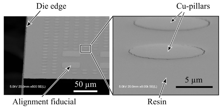
The test vehicles (TVs) employed in this work are provided by Resonac Corporation.: 1). Blank Si wafers coated with their proprietary resin (LB-2110) for conducting resin-to-resin bonding and adhesion experiments (schematically shown in Fig. 1(a)), and 2). Bumped Cu wafers coated with the half-cured resin and later CMP-ed to reveal the slightly raised (30 nm) Cu pillars (Fig. 1(b)). Both TVs employed 12-in wafers with a thickness of 775 µm. The Cu-pillar TV is designed to have round-shaped pillars having a diameter and pitch of 10 µm and 20 µm, respectively. The thickness of Cu pillars in TVs before and after CMP were 16 µm and 5 µm, respectively. The resin has a coefficient of thermal expansion (CTE) of 33 ppm/K and a glass transition temperature (Tg) higher than 350°C. Previous studies have reported the influence of average surface roughness Ra on the joint quality of TC bonded Cu pillars (Huang et al. 2022). The work by Huang et al. establishes that Ra should be in the range of a few nm to achieve void-free interface. The Ra of Cu pillars after the CMP process has been measured on the wafer level at five locations to be approx. 0.5 nm (n=3) using atomic force microscopy. Figure 2 shows scanning electron microscope (SEM) images of the diced die along with a blown-up image illustrating CMP-ed Cu pillars slightly protruding above the resin surface.
resin_tv_for_adhesion_test__and_(b)_cu-.png)
Bonding of both TVs is conducted in a ApturaTM TC bonder developed by K&S. The bonder consists of a nitrogen (N2) chamber that prevents formation of oxides on the target coupon when it is loaded on the thermal stage despite being at elevated temperature. All necessary calibrations related to vision, motion control and thermal budget are performed on the bonder before the experimental work. For bonding resin TVs, the coupons are manually placed and held by vacuum onto the thermal stage, which is moved inside the N2 chamber that maintains less than 100 ppm of residual oxygen. The top die is loaded onto a transfer shuttle (faced down) which presents it to the bond-head inside the N2 chamber. The bond head picks up the top die using a place nozzle that is an intermediate element allowing the bond-head to work with dies of various dimensions. In a typical TC bonding scenario, a vision subsystem utilizes pattern recognition to align the bumps and fiducials on both top die and bottom coupon. Subsequently, the bond-head is moved down to a so-called pre-clean height where formic acid vapor is applied for in-situ reduction of surface oxides on Cu surfaces right before TC bonding.
Design of experiments (DOEs)
First, the resin-only 4×4 mm2 dies are bonded to 8×8 mm2 coupons at various bond head and thermal stage temperatures as well as bonding pressures. Since there are no fiducials or patterns on the resin TV, bonding is carried out simply by instructing the bonder to place die in roughly center of the coupon. The purpose of this evaluation is to obtain a set of parameters that allows the resin-to-resin bonding without compromising its structure. In addition, a few samples were exposed to in-situ formic acid (FA) vapor before bonding to assess any adverse effects on the resin. After bonding, the samples were cross sectioned to optically judge the bonded interface. After bonding is established, more samples were prepared, and shear tests were carried out to establish the strength of the bonded interface using a Dage Series 4000 shear tester (Dage Precision Industries Ltd., UK).
For the Cu-pillar TVs, the top die (5.1×5.1 mm2) and bottom coupons (10.2×15.3 mm2) are similarly loaded onto the bond stage and transferred inside the N2 chamber. First, electrical pairing is performed by selecting bumps on the top die and corresponding bumps on the coupon. Next, pattern recognition is taught by using fiducials on the die and coupon with the help of an integrated vision subsystem. During bonding, the software aligns each top die before placing it on the bottom coupon using its individual DOE recipe-set. The parameters used in this recipe-set are listed in Table 1. After bonding, the samples were cross-sectioned and ion-milled to assess the joint quality. The parameters and their associated values used for TC bonding DOEs in the scope of this work are listed in Table 1.
III. Results and Discussion
Figure 3(a) shows a typical TC bonding profile where the force and temperature begin a ramp-up right after contact with the bottom coupon, labelled as step 1. In the next step, the bonding force and temperature are kept steady before ramping them down in the last step. Since there is no solder material that would otherwise require melting for joint formation, TC bonding for Cu-Cu application is relatively straight-forward and mainly relies on force as well as temperature to allow solid-state intermetallic diffusion to form a connection. Provided that Cu pillars across the TVs are in intimate contact with each other, the diffusion depth relies on the temperature and time (Wenzel et al. 2024).
_tc_bond_profile__(b)_optical_micrograph_of_a_cross-sectioned_resin-resin_bonded_sample.png)
Resin-resin bonding
At first, the bonding of Resin TV is evaluated using the parameters and procedure listed in Sec. II(b). The bonded samples were cross-sectioned, and the interface was examined for any gaps or cracks in both the resin and the Si base die. As shown in Fig 3(b), the bonded Resin TV shows no signs of cracking, delaminated interface or gaps. This specific top die has been bonded using bond force 100 N, bonding time 10 s and peak temperature 350°C while the bottom coupon experiences a stage temperature 100°C. The force and temperature ramps have been set to 200 N/s and 200°C/s, respectively.
Figure 3(c) illustrates the temperature profiles and z-position of five DOE-legs, highlighting the z-expansion of the sample as it progresses during bonding. In these plots, t=0 has been aligned with the start of temperature ramps of each DOE-leg after peak force is achieved. The plots may indicate that the partially cured resin tends to follow the temperature profile it is subjected to, and that the applied force does not have a significant effect on the z-growth. It is worth mentioning that stiffness of the bond head and its thermal expansion have been considered in establishing that actual z-expansion of the resin is only prominent at temperatures beyond 300°C. This is observable by the blue trace (Tpeak=350°C) with a gradual time-dependent z-growth compared to plateau in the green trace (Tpeak=200°C).
The resin TV evaluation with and without FA exposure prior to bonding has been further assessed by shear testing. The non-FA samples bonded using Tpeak=350°C and F=350 N sheared at σshear = 21.4±6.8 MPa (n=4). Samples bonded with FA vapor resulted with similar values of shear strength, verifying that FA vapor does not have any adverse effects on the resin-resin bond quality.
Cu-Cu TC BONDING
The bonding of Cu-pillar TVs utilizes bond head temperature profile from the resin bonding as a starting point; however, the stage temperature must be raised for establishing Cu joints based on our previous experience. In addition, any variation in the height of Cu pillars must also be considered, therefore, higher force values are selected for DOEs. Figure 4 shows SEM micrographs of attached Cu pillars for two different stage temperatures. Given that the resin is shallower than the Cu pillars, it is obvious that a tiny gap may remain and thus prevent resin from bonding completely if the temperature increase doesn’t balance the thermal expansion. Such gaps would not only fuel reliability concerns, but also make it favorable for ambient oxygen to penetrate and form Cu oxide during post-bond annealing process, as evidenced by an approx. 200 nm gap in the blown-up image in Fig. 4(a). In contrast, a higher stage temperature of 160°C enables more expansion in the resin on the bottom coupon (Fig. 4(b)), closing the gap and thus preventing any oxygen molecules to oxidize and risk degradation of the established Cu joints.
_sample_bonded_at_tstage_1.png)
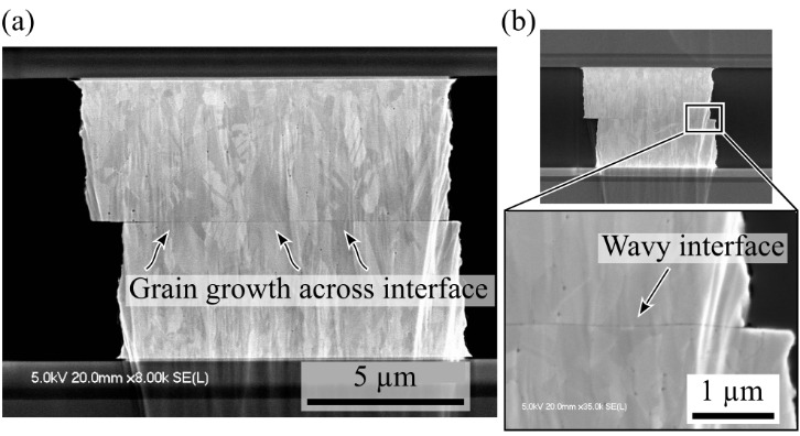
A successful Cu joint is typically characterized by the grain-growth across the bonded interface. Initial samples annealed for a shorter duration of 2 hrs did not provide enough evidence of grain-growth. Upon annealing the bonded sample for a 4x longer duration of 8 hrs at 250°C, ion-milled cross-sections revealed observable grain-growth across the interface as shown in Fig. 5(a). The absence of any oxide layer surrounding the Cu pillars additionally confirms good joint quality. Moreover, a blown-up SEM micrograph of an adjacent joint in Fig. 5(b) shows a wavy interface, which is a desirable outcome for properly attached Cu pillars (Martinez et al. 2013).
IV. Conclusion
The samples bonded in scope of this work demonstrate a single step process for attaching both Cu-pillars and the half-cured pre-applied underfill. The results of shear tests revealing an adequate amount of adhesion strength provided by the underfill. Furthermore, ambient-air annealing of samples prepared in this work showed no signs of unintentional oxidation of the Cu-pillars, which would otherwise be the case if any tiny gaps or voids were to remain as often seen when capillary underfills are used for small gaps. We believe that the high-accuracy TCB tool developed by K&S offering an in-situ oxide reduction using FA vapor is a tool of choice, and going forward, our approach of Cu-Cu TC bonding for fine-pitch applications can be readily adopted by the industry OSATs.
Acknowledgment
This work acknowledges the support of collaboration partners from Resonac Corporation who provided the test vehicles for conducting this demonstration.