

I. Introduction
In the rapidly evolving field of integrated photonics, the challenge of efficiently coupling broadband light between optical fibers and on-chip waveguides remains a critical bottleneck in the development and commercialization of photonic devices. Traditional methods of fiber-to-waveguide alignment often rely on complex and time-consuming active alignment techniques, which significantly increase production time, cost and limit scalability.
Optical sensors based on waveguides and various waveguide structures such as ring resonators and Mach-Zehnder interferometers have high sensitivity for detecting changes in the refractive index in the vicinity of the evanescent field (Duval and Lechuga 2015). These sensors normally require bio-chemical surface functionalization of the waveguides in order to have specificity to a particular compound of interest. This approach is particularly suitable for biosensing, where selective receptors are available. For sensing chemical molecules, e.g., benzene or ethanol, chemical surface functionalization can only provide some affinity, but not adequate selectivity for detection.
Alternatively, infrared spectroscopy can be used for direct detection of the desired compounds, without the need for surface functionalization because various chemical bonds absorb infrared light at specific wavelengths (“Infrared Spectroscopy,” n.d.). This fact significantly extends the lifetime of the sensors, provides faster detection capability and fast recovery times. Selectivity depends on the types of other compounds present in the sample to be analyzed. If the desired compound has a unique chemical bond, high selectivity is possible. In cases where many compounds have similar chemical bonds, it is more challenging. This is particularly true in the near-infrared region, 1 to 2.5 µm, where the infrared absorbance peaks are overlapping, less specific and less strong (Czarnecki et al. 2015). What makes this range highly desirable is the availability of optical fibers, light sources and detectors in the wavelength range.
Normally, dielectric waveguides rely on the evanescent field for sensing. However, due to short penetration depth into the surrounding medium and low density of gases, this approach is not sensitive and long waveguides are required for detecting low gas concentrations. To overcome the problem of low sensitivity and specificity for near-infrared detection of gaseous compounds, we developed a nanoporous-core silica waveguide, where the light propagating in the core directly interacts with the gas molecules entering the pores (Hutter 2020; Barua et al. 2023a). This provides improved sensitivity and ability to detect gases in parts-per-million (ppm) concentrations using an only 10 mm long waveguide.
The waveguide is transparent in the near-infrared spectral region and can be used for selective spectroscopic detection of gaseous compounds between 1 and 2.4 µm wavelength.
To improve the selectivity of detection, we introduced thermal modulation of the waveguide temperature which governs gas adsorption and desorption behavior in the porous core. Previously, we demonstrated with porous silica thin-films that adsorption and desorption depend on the characteristics of the gaseous compound such as its boiling point and its affinity to silica surface (Winter et al. 2021; Prestage et al. 2022; Day, Barua, and Hutter 2023). By monitoring gas sorption kinetics when cycling the temperature up and down, the adsorption and desorption kinetics can be attributed to a specific gaseous compound.
With respect to light coupling from fiber to waveguide, a grating-based light coupling is suitable when a narrow spectral range is used. For spectroscopic sensors, it is desirable to have a wide wavelength range as it allows for detection of multiple compounds and improved performance, thus butt-coupling is preferable. Previous studies reported various ways to achieve self-aligning of fiber-to-waveguide; tapered optical fibers inserted into buried channel planar waveguides (Gibson et al. 2005), U-grooves for aligning fibers to buried polymer waveguides (Wang et al. 2025), and V-grooves SiN edge couplers (He et al. 2019).
The overall sensor system reported in this work includes the waveguide chip, a Peltier element, a heat sink, and two optical fibers butt-coupled to the waveguide. Such system allows for temperature modulation between 5 and 70°C which is sufficient for adsorption and desorption of VOCs in and out of the nanoporous silica matrix (Winter et al. 2021; Day et al. 2023).
In this paper, we report on a self-aligned fiber-to-waveguide configuration that offers a robust solution for coupling fibers to waveguide without the need for active alignment. Our approach uses dedicated fiber-alignment structures adjacent to the waveguide, simultaneously fabricated, and made from the same material, thus eliminating the need for separate substrates, additional fabrication steps, and minimizing thermally induced optical misalignment.
II. Materials and Methods
Electrochemical Etching
A p-type boron doped silicon wafer with a resistivity of 0.01–0.02 Ω cm and < 100 > crystal orientation was electrochemically etched in a 1:1 mixture of 48% hydrofluoric acid (HF) and ethanol under a current density of 120 mA cm−2. The current was applied every 3 s for 2 s, and this was repeated for 1150 cycles, creating a 200 µm thick porous layer to act as the waveguide core. Then electrochemical etching continued at a current density of 130 mA cm−2 in a similar cyclic manner for 125 cycles, resulting in a 30 µm thick, porous layer to act as the waveguide cladding.
Waveguide Microfabrication
The microfabrication process steps are illustrated in Fig. 1. Following the electrochemical etching for silicon porosification (step 2 in Fig. 1), a silicon dioxide (165 nm SiO2) layer was deposited by sputter coating (step 3 in Fig. 1). The porous silicon samples were prebaked to drive off gas trapped in the pores prior to spin coating an 8 µm layer of AZ9260 (Merk) photoresist (step 4 in Fig. 1). In order to remove the edge bead, the pattern was masked, exposed to UV and then developed in AZ400K (Merk) (steps 5 and 6 in Fig. 1). The photoresist was then exposed through a precision chrome-on-glass photomask (JD Photo Data, UK) and developed in AZ400K again (steps 7 and 8 in Fig. 1).
Next, the samples are first etched for 3 minutes in octofluorocyclobutane (C4F8) to remove the exposed SiO2 layer. Then a Bosch style switched silicon etch process (McAuley et al. 2001) is used for deep reactive ion etching (DRIE) in an inductively coupled plasma (ICP) etch chamber to transfer the photoresist pattern into the porous silicon (step 9 in Fig. 1). Previous studies have shown that if the chamber has been carefully conditioned to reach equilibrium, then generally the run-to-run uniformity is within ±6% and our measurements, described later, fall within this range (McNie et al. 2003).
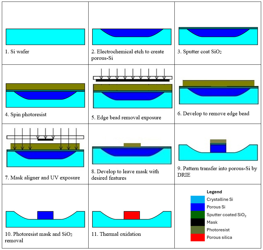
Following that, the remaining photoresist material and the SiO2 layer were removed using 50% HF 1:1 ethanol solution to expose the top surface of the waveguide (step 10 in Fig. 1). In the final step, the samples are thermally oxidized to porous silica (step 11 in Fig. 1) in a tube furnace under oxygen flow. The samples were heated at a temperature ramp rate of 1.6°C/minute to 300°C, held at that temperature for 60 minutes, followed by an increase to 800°C and further held for 960 minutes. This process converts the porous silicon matrix to porous silica matrix due to the open pore structure that allows oxygen diffusion throughout (Loni 2018).
Device Assembly
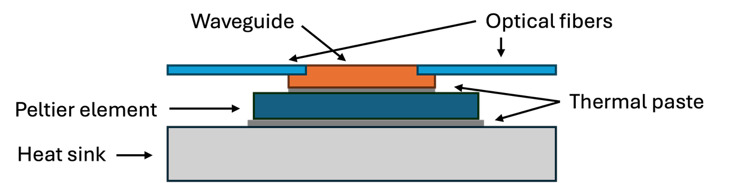
The waveguide chip was positioned on a Peltier element with an area of 20 mm by 20 mm and thickness of 3.8 mm (693-5078, RS Components). A temperature sensor with a 0.9 mm diameter (MP-2444, TE Technology) was mounted on the Peltier next to the waveguide chip in order to monitor and control the temperature. This was then placed on a heat sink. Thermal paste was used between the waveguide and the Peltier, and between the Peltier and the heat sink. Fig. 2 shows a schematic of the cross-section of the device.
Optical fibers (FG200LCC, Thorlabs) having a core diameter of 200 µm and a cladding diameter of 220 µm, were stripped of polymer coating and cleaved. The fibers were then inserted by hand into the alignment structures under a microscope. Once the fibers were positioned in place, a small amount of UV-curing optical adhesive (NOA61, Thorlabs) was applied to permanently secure the fibers.
III. Results and Discussion
A nanoporous silica waveguide requires a cladding layer of low refractive index between the silicon substrate and the (higher-refractive index) core of the waveguide. This is achieved by first etching the core of the waveguide for the required depth, then increasing the current density (which increases the porosity and hence reduces the refractive index) and continuing the etch until the required thickness of cladding has been achieved. The pore diameter (5-15 nm) is significantly smaller than the wavelengths used (0.5-2.4 µm) so both core and cladding can be regarded as homogenous materials as far as the propagation of light is concerned. The duration of the etches was chosen to match (once oxidized) the core and cladding thickness of the fiber used.
DRIE was used to remove the unwanted porous silicon material and leave just the desired features – namely the waveguide and the alignment features for the optical fibers. Rough sidewalls increase optical loss of the waveguide, as does a concave waveguide cross-section, so the etch process was designed to be as anisotropic as possible (92-94°) with minimal roughness. An ICP etch chamber has several advantages compared to other plasma sources like RIE, principally, because of its greater scalability and wider operating window and was necessary in order to achieve the near vertical smooth waveguide profile that was required. The silicon etch process consists of a sequence of alternating etch and passivation cycles. The passivation and etch gases used were C4F8 and sulfur hexafluoride (SF6) respectively. The passivation phase deposits a fluorocarbon polymer over all surfaces of the wafer and trenches. During each etch cycle, the passivation is removed from the bottom of the etched features with the assistance of ion energy. The rest of the etch cycle is a short isotropic etch of the exposed silicon. As the vertical etch rate significantly exceeds the lateral etch rate, the sidewall profile is a lot more anisotropic compared to the previously used RIE process. Multiple parameters were varied to tune the process including the coil power, the platen power and duty cycle, the gas flow rates and switching times, the platen height and temperature, the chamber pressure, as well as the exposed Si area on the chip. This silicon etch process was uniquely tailored to avoid damage to the pores to maximize waveguide efficacy of coupling and reduce optical losses. Average etch rates of 17 µm/min were achieved with a uniformity of ±1.3 %.
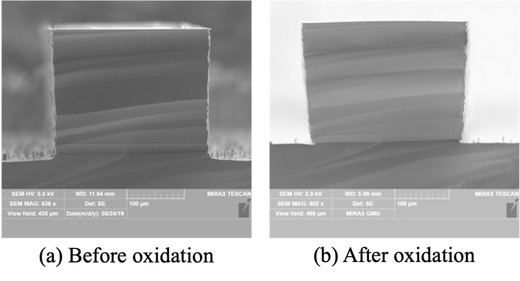
Thermal oxidation is used to convert the porous silicon to porous silica, resulting in an expansion of the waveguide and the alignment features, and strain between these features and the underlying silicon wafer. Fig. 3 shows cross sectional SEM images of waveguide before and after thermal oxidation.
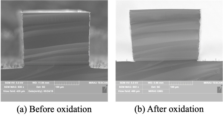
The etch depth was 274.43 ± 0.99 µm and the side wall angle was 92.84 ± 0.87°. The width of the waveguide as etched was 176.44 ± 2.21 µm at the top, which expanded to 193.56 ± 1.92 µm after thermal oxidation. At the base, the width remained similar (149.21 ± 6.17 µm before and 150.65 ± 4.65 µm after). The extent of width increase at the middle of the waveguide height is similar to that at the top of the waveguide. The data is summarized in Table 1 showing the waveguide width at the top, middle and the base of the waveguide, demonstrating the extent of the expansion due to thermal oxidation which converts the porous silicon matrix to porous silica. Such complete oxidation is possible due to the open pore network of the porous matrix facilitating oxygen diffusion.
The expansion of the waveguide width is about 9% at the top of the waveguide and the alignment features, which has to be taken into account in the mask design. Towards the base of these structures the expansion is much smaller as the underlying crystalline bulk silicon substrate does not appreciably oxidize and thus constrains the expansion. Due to this volume change, the distance between the alignment structures must be carefully tailored to match the outer diameter of the optical fibers, ensuring a snug fit and precise alignment with the waveguide core dispensing with the necessity for active alignment. Tests were done for system reliability and dimension tolerance between multiple runs was found to be ±2% after the silicon etch process. After the HF strip, it is ±4% and after the oxidation it increases to ±6%.
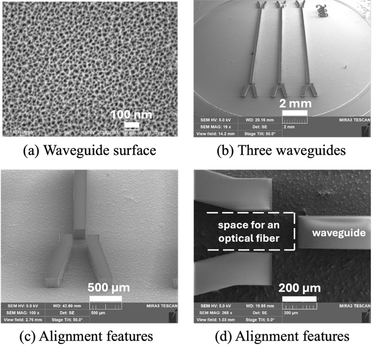
The image of the porous waveguide surface is shown in Fig. 4(a). Because the pore sizes are much smaller than the wavelength of light, light can propagate without significant scattering losses. The final chip comprises an array of three waveguides, each with a width of ~195 µm, with their accompanying alignment features at each end as shown in Fig. 4(c-d).
_sem_image_of_the_porous_waveguide_surface_from_the_top__(b)_the_whole_sample_showing_an_.png)
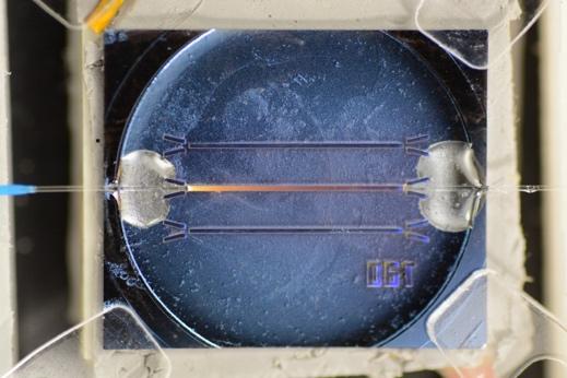
Fig. 5 shows a photograph of the optical fibers aligned with the middle waveguide, which were then further secured by the adhesive. White light entering the waveguide form the left fiber can also be seen in the image.

Estimation of the optical misalignment loss was done based on the geometry of the fiber and the waveguide, and assuming the light intensity across both is uniform. The calculated transmission loss for light passing from the fiber to the waveguide and into another fiber is 19.4%. Misalignment of either interface by 10 µm would lead to an additional loss of up to 2%, rising to up to 6.1% at 20 µm misalignment.
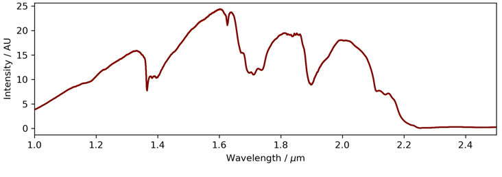
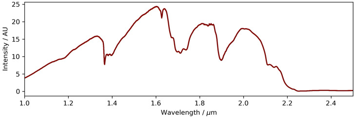
A fiber coupled Fourier-transform near-infrared spectrometer (Antaris MX FT-NIR, Thermo Scientific) was used to acquire the near-infrared spectra between 0.9 and 2.5 µm with 128 scans at 4 cm-1 resolution. The transmission spectrum through the waveguide is shown in Fig. 6. High light absorption is seen for wavelengths higher than 2.2 µm which is expected for silica. Absorption around 1.4, 1.7 and 1.9 µm is attributed to Si-OH and OH bonds. Overall, good transparency is observed in the near-infrared spectral range.
Sensing capability of the nanoporous waveguide can be demonstrated by exposing it to a gas and measuring the infrared absorption peaks corresponding to the chemical bonds of the gas molecule.
First, the transmission spectrum through the waveguide was measured when the waveguide was exposed to dry air at a waveguide temperature of 70°C. At this condition, it can be assumed that there are no compounds present in the waveguide’s pores, and this spectrum is used as a reference for absorption calculation. Then, the waveguide was exposed to 10 ppm of propan-2-ol (isopropyl alcohol, IPA) vapor and the temperature of the waveguide was reduced to 5°C. Wavelength dependent absorbance is then calculated according to Beer-Lambert Law (“The Beer-Lambert Law,” n.d.):
\[Abs(\lambda) = \log_{10}(\frac{I_{reference}(\lambda)}{I_{sample}(\lambda)})\]
where is the spectrum of waveguide in dry air, is the spectrum of the waveguide when exposed to the gas, and is the wavelength of light.
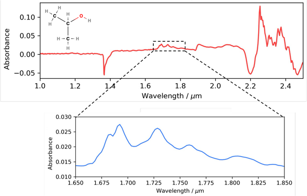
Fig. 7 shows the near-infrared absorbance spectrum of 10 ppm IPA at a waveguide at 5°C. On the top left side, the molecular structure of IPA molecule is provided, and in the bottom, a zoomed-in view of IPA’s characteristic absorbance peaks between 1.65 and 1.85 µm is shown.

The absorbance peaks between 1.6 and 1.8 µm and between 2.2 and 2.4 µm are associated with CHx groups of the IPA, while the peaks around 1.9 µm and between 2 and 2.2 µm are associated with the OH group (Weyer 2012). This confirms the direct measurement of IPA molecules in the pores of the waveguide.
There are also two negative absorbance peaks around 1.37 and 2.20 μm. Negative peaks appear when there is a decrease in the number of a particular chemical bond compared to the reference spectrum. These two peaks most likely correspond to OH bonds of the porous silica - upon hydrogen bonding with IPA (i.e. the interaction of Si-OH with IPA’s OH), there is a decrease in the number of Si-OH that interact with air. And because the wavelength at which OH vibrates changes depending on whether OH is surrounded by air or other molecules, these negative peaks are expected.
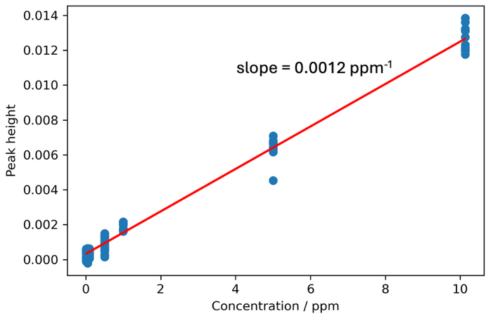
Sensing behavior of the waveguide is demonstrated by measuring eight different IPA concentrations between 12.5 parts-per-billion (ppb) and 10 ppm, ten repeats each. The peak height is calculated by taking IPA’s peak absorbance value at 1.69 µm and subtracting absorbance value at a baseline near the peak at 1.65 µm. A graph of peak heights versus concentration is shown in Fig. 8. A detection limit of 1.76 ppm was calculated as three times the standard deviation of the peak height of the blank sample (0 concentration) divided by the sensitivity, which is defined as the slope of the calibration curve. This excellent sensitivity shows an orders of magnitude improvement compared to standard near-infrared free-space spectroscopic gas analysis (Barua et al. 2023a).

The waveguide provides means to perform near-infrared spectroscopic analysis of organic compounds entering the nanopores of the waveguide, where their infrared spectral features resemble those of molecules in liquid-phase (Barua et al. 2023b). The ability to detect multiple compounds simultaneously, or a specific compound in a mixture, depends on the particular spectroscopic features of the compounds. For example, our previous study demonstrated simultaneous measurement of toluene and 1-octene adsorbed in the waveguide (Barua et al. 2022).
IV. Conclusions
A novel nanoporous silica waveguide sensor has been designed to operate in the near-infrared spectral range. In order to ensure stable optical light coupling to the waveguide under a range of temperatures and to provide efficient and passive alignment of the optical fibers with the waveguide, self-aligning features for the optical fibers were simultaneously fabricated. The alignment features are defined on the same mask as the waveguides, ensuring accurate positioning with respect to the waveguides. Following thermal oxidation of porous silicon to porous silica, the waveguide and the alignment features expand in volume which required optimization of the mask dimensions.
The close mechanical coupling of waveguide and fibers via the alignment features positioned on the same silicon substrate as the waveguide ensures good mechanical and thermal stability. These alignment features are also designed to facilitate easy insertion of the fibers and provide a structure against which the fibers can be glued to provide further mechanical support. This design facilitates straightforward insertion of fibers which can be done manually under a microscope, thus eliminating the need for active alignment, expensive instrumentation, and therefore reducing the time and cost for manufacture of the sensors.
The porous silica waveguide sensor with the optical fibers provides transparency in the 1 to 2.2 µm wavelength range, enabling highly sensitive near-infrared spectroscopic gas analysis. Its gas sensing capabilities were demonstrated using IPA at concentrations up to 10 ppm, achieving a detection limit of 1.76 ppm, thereby confirming its suitability for gas sensing applications.