
I. Introduction
Artificial intelligence, big data and complex modeling require efficient high-performance computing modules. In addition to the development of ICs that can perform individual computing operations with high efficiency and speed, the interconnection of these chips to their environment is also one of the main challenges of high-performance computing (HPC).
For instance, short transmission paths between computing and memory chips and high signal integrity are required to take full advantage of a leading-edge chip architecture. Advanced packaging is therefore a central building block for the realization of HPC modules. One option for the advanced packaging of HPC modules is the integration of computing and memory chips in a single System-in-Package (SiP) (Matsuo et al. 2000; Lau 2021; Bhattacharya and Rao 2023). In addition to the integration of one computing and memory chip each, such a packaging platform can also enable the integration of a larger number of chips or chiplets and thus also makes a significant contribution to the emerging chiplet infrastructure.
According to this approach of heterogeneous integration in a SiP, one or more ICs that are optimized for specific computing operations such as stencil processing units (Datta et al. 2008; Krüger et al. 2011; Donofrio et al. 2009) or GPUs can be assembled together with High Bandwidth Memories (HBM) on a silicon interposer (Chidambaram 2019; Wang et al. 2023). Interposers and chips are connected with microbumps with a pitch in the range of 50 µm (Lee et al. 2018). In addition to the use of silicon as interposer material, glass and organic interposers, possibly with integrated glass or silicon bridges, can also be considered (Li et al. 2016; Usman et al. 2017). Silicon interposers are currently wide-spread due to their ability to support high density wiring and existing process lines.
For the packaging of such HPC modules in a high-volume production, wafer level processes such as redistribution layer (RDL) processing and compression molding are key technologies. While wafer level packaging imposes major advantages such as good scalability, it also includes challenges such as warpage that increase with the size of wafers (Braun et al. 2024, 2023b; Braun and Hoelck 2022) which have to be addressed in a proper process evaluation.
II. Process Flows for HPC Modules
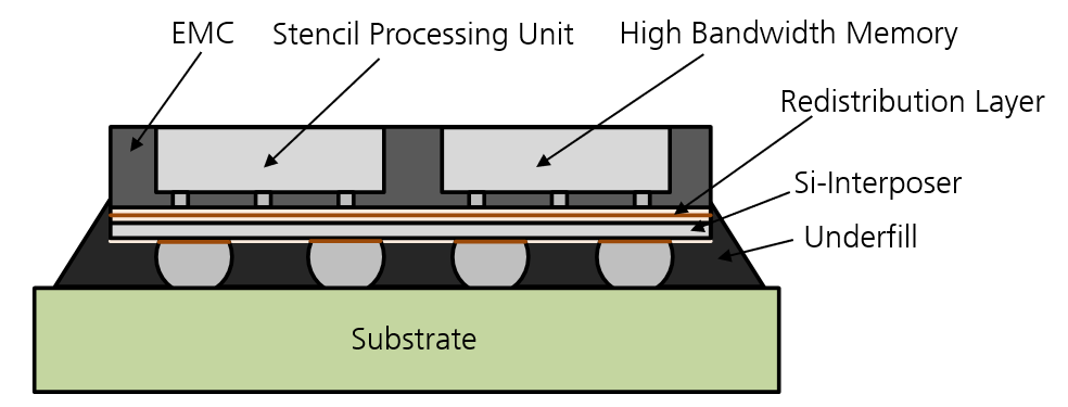
In order to investigate the manufacturing of an HPC module with the previously described setup of processing unit and HBM on silicon interposers and to analyze optimal process control, a simplified demonstrator setup is developed (Figure 1). A stencil processing unit and an HBM are integrated on a silicon interposer. In subsequent development steps, the platform can be extended to integrate a larger number of chips on an interposer using the chiplet approach.

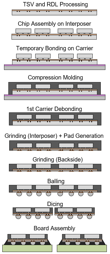
To set up the demonstrator module, the HBM and the processing unit, each with a thickness of 725 µm, are mounted on an interposer. The gap defined by the bump height with a distance of 35 µm between interposer and chips. It can either be filled with an underfill for thermo-mechanical stabilization or the underfilling is integrated into the encapsulation process by compression molding in the so-called molded underfill. The interposer wafer initially has a thickness of 725 µm. After thinning the wafer and exposing the through silicon vias (TSV), the final thickness is 100 µm. The thinning and complete processing of the interposer can take place either before or after compression molding. These two possible process variants are shown in Figure 2 and Figure 3. The 200 mm interposer wafer is fully processed before molding, including thinning and pad generation, in the process flow shown in Figure 2, and subsequently molded with a cap of 190 mm diameter, using the rim of the wafer for the sealing of the mold cavity. During this process, a glass carrier can be used to stabilize the 100 µm thin interposer. Handling during the balling process allows flexible wafer size, so the thin rim of the interposer wafer can be removed by sawing after carrier debonding to avoid uncontrolled fracturing.


For the process flow shown in Fig. 3, further process steps such as pad generation are necessary after molding. For these processes, a standard wafer size such as 200 mm is mandatory for handling and machine processes. Thus, the interposer wafer is cut down to 190 mm before molding to so that a 200 mm wafer can be molded. This allows handling of a stable 200 mm wafer without the necessity to remove a thin rim as in the first process flow.
The finished module has a size of 25x15 mm² and is assembled to an organic substrate after solder balls have been applied. The ball grid array layout is based on current standards; typical ball sizes are around 300 µm and typical pitches are 500 µm (“IPC 7095 - Design and Assembly Process Implementation for BGAs,” n.d.). Here, too, underfilling and the mounting of a heat sink or lid with suitable thermal interface material on the back of the module for optimized heat dissipation follow.
The limit for further processing of the encapsulated wafers in the balling process at IZM is typically 2 mm total warpage for a mold wafer with d = 200 mm; the aim of process development is to remain below this threshold value. A holistic assessment of the whole process chain is carried out to secure a high performance and reliability of the HPC packaging platform.
III. Interposer Layout and Processing
To provide sufficient high wiring density for the interconnection of computing and memory devices on interposer, Fraunhofer IZM has further developed its multi-layer routing technologies (Zoschke et al. 2024). The multi-layer routing technology is originally adapted from well-known redistribution technology for fan in wafer level packaging featuring electroplated copper for the wiring and thin film polymer as intra- and interlayer dielectric. Standard redistribution technology typically has relaxed wiring density with 5 µm thick copper lines having minimum 12 µm lines/space and large vias in 10 µm thick polymer, realized by direct lithographic structuring using a photosensitive polymer.
However, for the interconnection of ICs with high IO-density, a higher wiring density is needed. To meet this requirement, the multi-layer routing technology has been scaled towards higher density during the last couple of years.
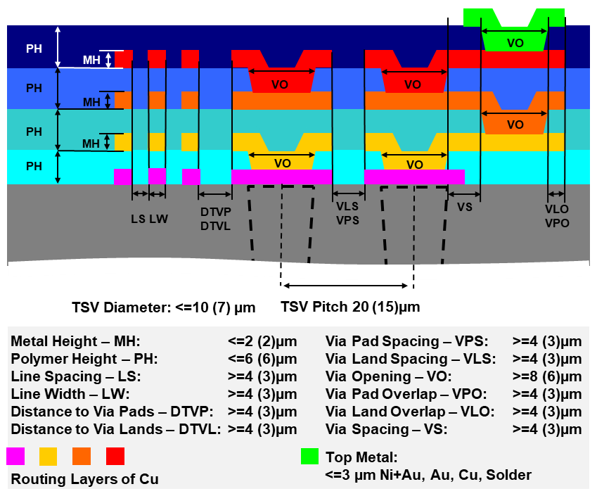
Routing on an interposer device for HPC applications has to reach densities of 4 µm lines and space and beyond to meet the interconnection requirements of typical compute and memory chiplets. The required upscaling of routing density was enabled by reduction of layer thickness for copper and polymer. Thinner layers allow use of thinner photo resists and reduce final warpage, so that finer structures are possible for both, wiring and vias.
With a restriction of the maximum copper height to 2 µm per layer and maximum polymer thickness to 6 µm per layer, the layout rules shown in Figure 4 were defined. Based on that, a line pitch of 8 µm with symmetric width and spacing of 4 µm is possible over multiple layers. The polymer vias, which are generated by laser ablation using a pre-defined hard mask, were defined with a diameter of 8 µm. Secondary layout rules such as overlaps and via spaces can be also found in Figure 4. As it can be seen in the picture, the design rules support a possible TSV pitch of 20 µm for the interposer device. All numbers in brackets refer to the next technology release which can support a routing scenario of 6 µm pitch (3 µm lines and space) to support a 15 µm TSV pitch in the interposer device.

All pattern definition steps are done by mask aligner lithography and thin photo resists. Lithography based on mask aligner is a feature of this technology, because it is especially useful for realization of large devices which exceed typical stepper reticle sizes, so that no reticle stitching is required. In extreme cases full wafers can be re-routed and finally used as one device (Zoschke et al. 2017). Details of the process, especially related to the direct laser structuring approach of the polymer vias are described in (Zoschke et al. 2019).
IV. Encapsulation by Compression Molding
A. Compression Molding and Warpage
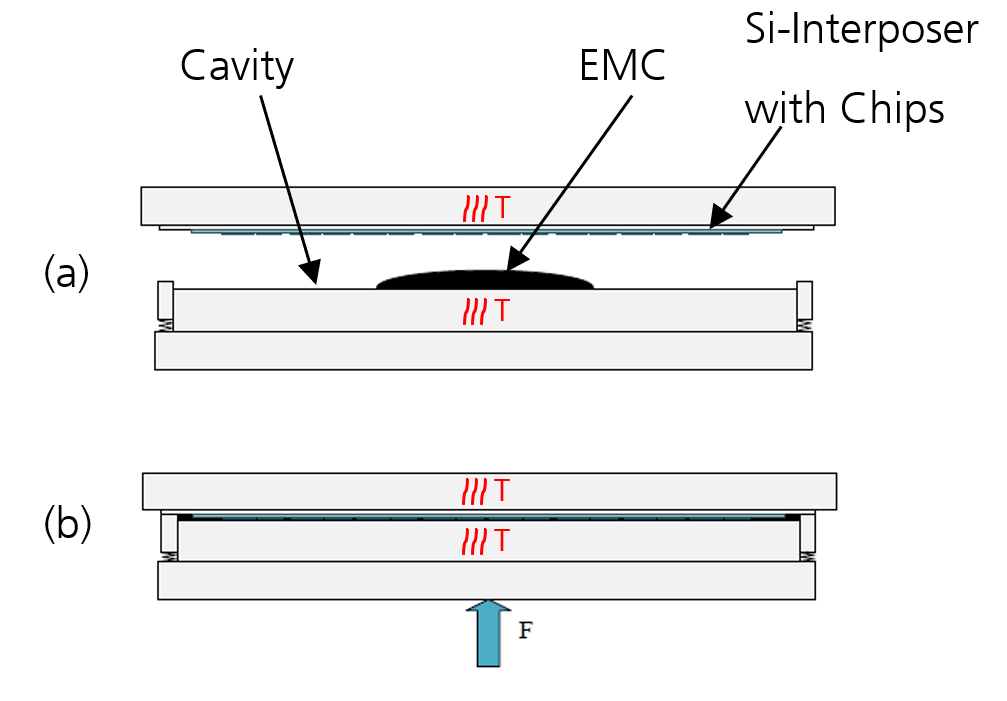
Compression molding is a well-established process for large-area encapsulation in the area of wafer level and panel level packaging in volume production (Braun et al. 2023a). A variety of mold system suppliers are offering equipment for these processes, for this study a TOWA compression molding system in cavity down configuration has been used. For encapsulation at wafer level, an epoxy molding compound (EMC), an epoxy-based polymer filled with SiO2 particles, is dosed into a cavity in wafer form (lower half of the tool). The components to be encapsulated are then placed on a carrier in the open mold (upper mold half), the mold is closed, the cavity is evacuated and the EMC is pressed into the cavity by moving the mold onto the component carrier (see Figure 5). The EMC hardens under pressure and temperature during the In-Mold Cure (IMC) and achieves sufficient mechanical strength to be removed from the cavity. The final cross-linking takes place in a subsequent post-mold cure (PMC) in an oven outside the cavity.
_placing_interposer_and_emc_in_cavity__(b)_closing_ca.png)
The epoxy molding compound must have a sufficiently high flowability for processing in compression molding in order to fill the entire cavity and all gaps between the components without voiding. In particular, in order to achieve the narrow gaps between chips and interposer as a molded underfill, small filler sizes and low viscosity are required at the same time. The materials shown in Table 1 were selected for the process discussed here. Material C in particular is characterized by a small filler size, but at significantly higher costs than materials A and B.
In addition to the electrical insulation of the individual contacts (e.g. whisker formation, short circuits due to conductive contamination), the EMC also serves to mechanically reinforce the assembled components under operating conditions, both during further processing and in the subsequent application. Therefore, sufficient material stiffness is required for stabilization and good thermo-mechanical adaptation of the EMC to the other materials present in the package. However, excessive stiffness can be critical, as warped wafers can no longer be processed if the stiffness is too high, for example if vacuum chucking and therefore processing of the warped wafer is not possible.
In order to keep warpage generally low, the CTE of the EMC should deviate as little as possible from the CTE of the silicon interposer (2.6 ppm/K). A difference in the CTE creates internal stresses when cooling from the processing temperature, resulting in warpage of the wafer at handling temperature. Since polymers generally have a significantly higher CTE than silicon, a low CTE is an important target value when selecting the EMC. Since the exact warpage and its limits depend on a variety of parameters such as stiffness, CTE and component structure, the warpage after compression molding and the processability of the warped wafers are analyzed in the experiment.
B. Experimental Design of Molding Study
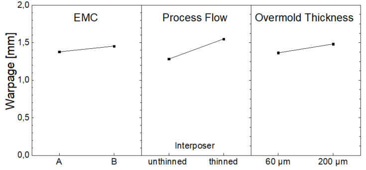
To compare the process variants presented above, the process is run through as a demonstrator production. In order to also consider warpage as an important quality criterion, a test plan is developed in which the molding compound and the overmold thickness are examined as parameters in addition to the two variants of the process flow. The choice of material and the overmold thickness can potentially have a decisive influence on warpage, as they determine the degree of contraction of the upper layer of the structure and thus the internal stresses introduced.
The parameters of the full factorial test plan are shown in Table 2. The more cost-effective material variants EMC A and B are examined first.
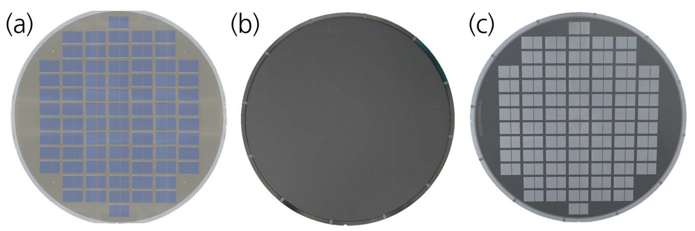
For this demonstrator run to investigate the mechanical behavior, dummy chips made of silicon are mounted with a die attach material on the silicon wafers, which serve as interposers (Figure 6). This structure deviates from the final product, where the interposer is covered by a multi-layer RDL and chips are connected to the RDL with bumps, the bulk
_mounting_the_chips_on_interposer__(b)_molding__(c)_backgrinding_to.png)
Compression molding is carried out using a Y-120 wafer molding machine (TOWA, Kyoto, Japan). The material manufacturer’s recommendations according to Table 1 are used as the processing temperature and time. Directly after molding and after each process step, the warpage is measured using a precision 3-coordinate measuring system (OMS 600, Mahr GmbH, Göttingen, Germany).
C. Evaluation
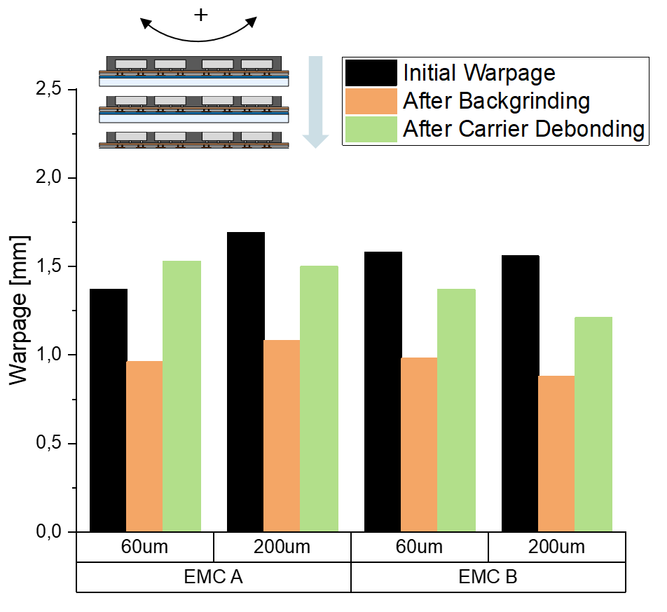
After molding, a warpage of the wafers in the range of 1.1 mm to 1.7 mm results for all process variants. The most pronounced effect on warpage can be observed for the factor process flow (Figure 7). A significant difference is reasonable due to the different mechanical structure. However, since additional steps for processing the interposer follow for the unthinned interposers, even a lower warpage can also be critical here.
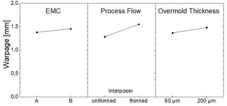
The other parameters examined, EMC and overmold thickness, have a less significant influence on warpage. The slight increase in warpage associated with thicker overmold thickness is generally plausible, as more EMC also leads to greater stress due to the greater contraction of the upper layer of the package structure when cooling from the processing temperature. Although the average warpage values for both types of EMC are similar in the initial state, some differences become apparent especially after the following process steps.
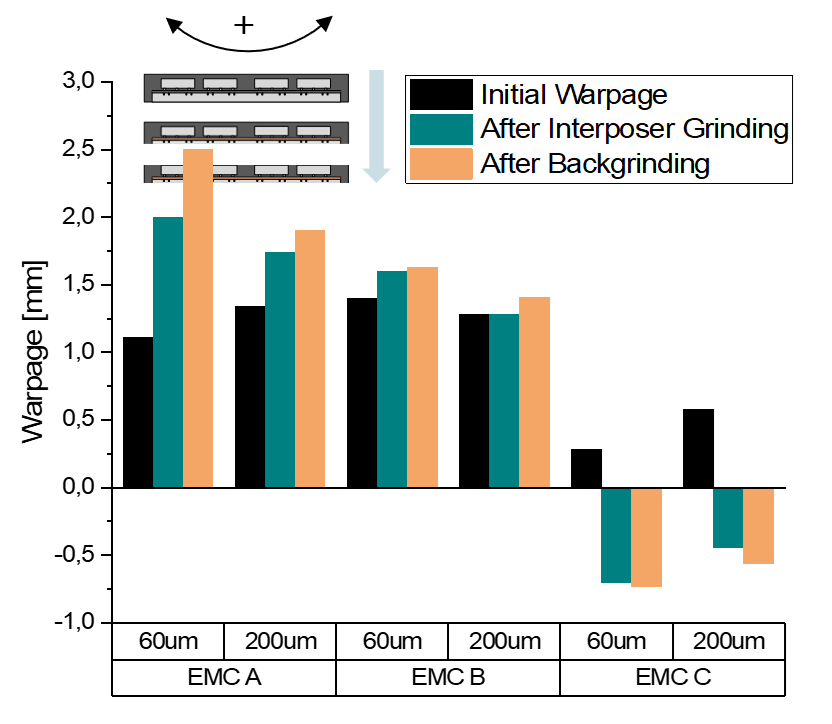
In the further investigation of the first process flow, in which not yet fully processed interposers are overmolded, an increase in warpage can be seen for almost all of the wafers examined after the interposer has been thinned and the backside subsequently ground (compare with Figure 3). This can be explained by the decrease in the stiffness of the overall structure.

Grinding of the backside to reveal the die backsides could have the effect that stress is reduced since the layer of plain EMC with comparably high CTE is removed. However, the fact that backgrinding causes an increase in warpage can be explained by a further decrease in stiffness, while internal stresses generated by the surrounding ring of EMC around the interposer remain. Interestingly, this behavior is more pronounced for EMC A, even though its CTE is lower compared to EMC B. Other factors such as high mechanically relevant shrinkage and low stress additives (LSA) may have an impact on this effect.
Further processability proves to be problematic with this process variant; for example, the suction of the wafer to oxidize the bottom side of the interposer is not possible with the system used.
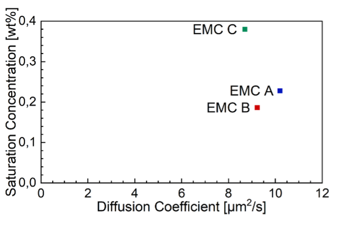
EMC C is tested as a possible alternative material. Figure 8 shows that a significant reduction in warpage can be achieved. After thinning the interposer, the measured warpage is negative, i.e. the wafer is warped in the direction of the interposer. This can possibly be explained by the expansion caused by the absorption of moisture. A higher maximum moisture absorption is supported by material analysis, that shows a significantly higher saturation concentration of water in EMC C compared to the other materials, even though the diffusion coefficient, indicating the absorption kinetics, is lower. Figure 9 displays these values, gained from dynamic vapor sorption analysis with a Discovery SA (TA Instruments, New Castle, DE), see (Braun et al. 2015) for meterology.

For the process variant in which already processed interposer wafers are overmolded (cf. Figure 2), there is a clear reduction in warpage after the chip backsides have been exposed by grinding (Figure 10). This decrease is expected, as the tensile stress from the “pulling” EMC layer is relieved. Following debonding of the encapsulated wafer from the glass substrate—onto which the thinned interposer was originally mounted for processing—an increase in warpage occurs again, as anticipated, due to the reduced structural stiffness.
At no point in the process were issues observed with wafer handling via vacuum suction. This indicates that the process flow is advantageous compared to the previously described variant, despite the higher initial warpage after molding.

The process variant using a pre-thinned and completed interposer meets the <2 mm warpage requirement for balling for both molding compounds used, and is further considered lower risk, as sensitive steps such as the final processing of the interposer’s bottom side are no longer required on an already warped, molded wafer.
This process flow was successfully validated in experiments using both materials A and B, as well as with both tested overmold thicknesses (60 µm and 200 µm). To further reduce the warpage without considering the material costs, the use of EMC C is also possible here, but not necessary.
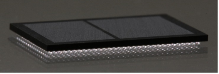
Figure 11 shows an example of a module after molding, backgrinding, application of solder balls and dicing.

V. Conclusion and outlook
HPC modules require a suitable packaging platform to enable communication between multiple chips and to protect the components. Such a platform ranges from interposers with high-density electrical redistribution layers and solutions for encapsulation to balling and mounting on a substrate. The work presented here deals with suitable processes for the production of HPC modules with a focus on encapsulation. Encapsulation by compression molding is suitable for increasing the robustness of the interposer wafers during the process and for meeting the reliability requirements for assembly and operation in the application. However, the encapsulation process also introduces a warping that influences handling in the subsequent process steps or makes it impossible if the warpage is too large. With sufficient knowledge about the factors influencing the warpage, about the change in warpage during and after the respective process steps and about the limits of tolerable warpage, optimized parameters for the encapsulation process can be found. In the investigations carried out for this purpose with non-functional components, the process variant in which compression molding is carried out on a thinned interposer wafer was successfully demonstrated up to balling and separation, and both EMCs used were qualified as suitable encapsulation materials.
The next step is to investigate the molded underfill of the gap between the chip and interposer. In parallel, work on the simulation, design and construction of functional interposers with high-density redistribution layers is ongoing and the effect of warpage and stress on package level after the assembly on board has to be evaluated.