


(1) Introduction
Some of the early research of glass in semiconductor packaging dated back almost 20 years ago. For example, the flip chip on glass substrate has been studied by Loughborough University (Bhatt et al. 2007; Cui et al. 2007). At Fraunhofer IZM, they have studied: (a) a thin glass based packaging technology for optoelectronic modules (Brusberg, Schroder, Topper, Arndt-Staufenbiel, et al. 2009), (b) a glassPack SiP uses thin glass foils as substrate material (Brusberg, Schroder, Topper, and Reichl 2009), (c) a photonic SiP technology using thin glass substrates (Schroder et al. 2010), and (d) 3D glass interposer for system-in-package (SiP) with integrated optical interconnects (Topper et al. 2010). Georgia Institute of Technology (GIT) have done the most research in applying glass to semiconductor packaging, e.g. (S. Kim et al. 2024; Sukumaran et al. 2010; Tummala et al. 2011; Sukumaran et al. 2012; McCann 2014; Ravichandran et al. 2020; Wong et al. 2020; Ali et al. 2020; Erdogan et al. 2021; Sivapurapu et al. 2021; Huang and Swaminathan 2021; Jayaram, Gupte, and Smet 2022; Jia et al. 2022; Ravichandran et al. 2022; J. Kim et al. 2023; Li et al. 2023; Kathaperumal et al. 2024; Molina-Mangual et al. 2024),. Another well-known company which has been working on applying glass to semiconductor packaging is Corning Research & Development Corporation, e.g. (Bowrothu, Yoon, and Zhang 2018; Hwangbo, Yoon, and Shorey 2018; Okoro, Allowatt, and Pollard 2021; Pan, Xu, and Park 2021; Pan et al. 2022; Yeary et al. 2023; Brusberg et al. 2024; Yang et al. 2024),.
Some of GIT’s research is shown in Figure 1 (Sukumaran et al. 2010; Tummala et al. 2011; Sukumaran et al. 2012; McCann 2014; Ravichandran et al. 2020; Wong et al. 2020; Ali et al. 2020; Erdogan et al. 2021; Sivapurapu et al. 2021; Huang and Swaminathan 2021; Jayaram, Gupte, and Smet 2022; Jia et al. 2022; Ravichandran et al. 2022; J. Kim et al. 2023; Li et al. 2023; Kathaperumal et al. 2024; Molina-Mangual et al. 2024). It can be seen that the organic-core build-up package substrate, Figure 1(a), has been replaced by the glass-core build-up package substrate, Figure 1(b). Also, the traditional TSV-interposer (Lau 2013) has been replaced with the through-glass via (TGV)-interposer, Figure 1(c) – a 2.5D IC integration. Finally, they embedded a chip such as the static random-access memory (SRAM) in the glass-core build-up package substrate – a 3D IC integration, Figure 1(d).
Absolics Inc., a US subsidiary of South Korean Chaebol SK Group (SKC) in Georgia, which is in tight cooperation with GIT, will be in high volume manufacturing of the glass-core package substrate and the TGV-interposer in 2026 (2024).
_organic-core_package_substrate._git_s_semiconductor_packaging_with_glass__(b)_glass-core.png)
On September 18, 2023, Intel announced they will use the glass-core substrate to replace the traditional organic-core substrate for their one-trillion transistors processors to be shipped before 2030 (2023).
On April 23, 2025, during the TSMC 2025 North America Technology Symposium (April 23), the company announced its chip-on-panel-on substrate (CoPoS) to replace some of their chip-on-wafer-on substrate (CoWoS) for high-performance computing (HPC) driven by artificial intelligence (AI). The CoPoS products are planned to be shipped in late 2028 and the glass panel size is 310mm x 310mm.
(2) Motivation
By now, reliability issues because of the glass-core substrate are seldom discussed, especially the semiconductor packaging interconnects such as the solder joint reliability.
The trends of flip chip interconnects are shown in Figure 2 (Lau and Fan 2025; Lau 2024a, 2025, 2024b, 2023, 2022). It can be seen that the size (diameter) as well as the pitch of the interconnects are from large to small. A few years from now, in some niche applications such as the one trillion transistors processor, the pad pitch and pad size could go down to < 20µm and < 10µm, respectively.

_organic-core_substrate._(b)_glass-core_substrate___4902.png)

In this study, the solder joint reliability of semiconductor packaging, because of the glass-core substrate, is investigated and there are two problems. One is shown in Figure 3 for high-performance and high-density products, and the other is shown in Figure 4 for extremely fine-pitch, high-performance and high-density niche products such as the one-trillion transistors processors. The fabrication process of TGV and redistribution-layers (RDLs) will be briefly mentioned first.
_process_flow_of_tsv._(b)_sem_image_of_a_tsv.png)
_process_flow_of_tsv_rdls._(b)_l_s__2m._(c)_l_s___lt__2m.png)
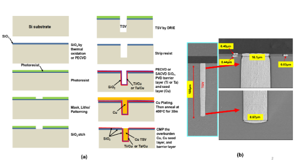
The fabrication process of TGV is very different from that of TSV. Most of the TSVs are fabricated by the deep reactive-ion etching (DRIE), Figures 5 and the RDLs by Figure 6. However, today most of the TGVs are fabricated by laser drilling such as the laser induced deep etching (LIDE) developed by LPKF Laser & Electronics AG in 2017 (Ostholt, Ambrosius, and Kruger 2014; Xing et al. 2025; Chen et al. 2025). The most common used glass materials are the SCHOTT AF 32 alkali-free flat glass and the CORNING HPFS 7980 high purity non crystalline fused silica glass. Both materials have low coefficient of thermal expansion (CTE), which are close to that of silicon.
_fabrication_process_flow_of_tgv._(b)_sem_image_of_a_fgv._(c)_etch_solution_mechanism.png)
_sidewall_metllization._(b)_cu_plating._(c)_sem_image_of_a_cu-filled_tgv.png)
_l_s__2m._(b)_l_s____2m.png)
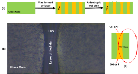
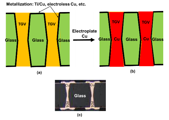
The process flow for fabricating the TGV is shown in Figure 7(a). It can be seen that the vias are formed by high-speed laser and the modified area of the glass are removed by anisotropic wet chemical etching, e.g., hydrofluoric acid (HF) or sodium hydroxide (NaOH). Figure 7(b) shows a typical TGV. It can be seen that there is a taper angle of the TGV. This is due to the rate of the circulation and temperature of the etching solution, and the concentration difference of the etching solution to make the outer ionizer move inward and replenish as shown in Figure 7(c). The higher the etching rate the larger the taper angle. It is followed by the metallization of the seed layer such as Ti/Cu, electroless Cu, etc. as shown in Figure 8(a). Then, electroplate the Cu to fill the via as shown in Figure 8(b). Figure 8(c) shows an SEM image of the Cu-filled TGV.
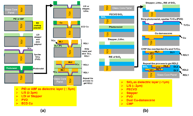
The process flow for fabricating the RDLs of the TGV is very similar to the RDLs of TSV (Figure 6) and is shown in Figure 9(a) for L/S ≥ 2µm and Figure 9(b) for L/S < 2µm.
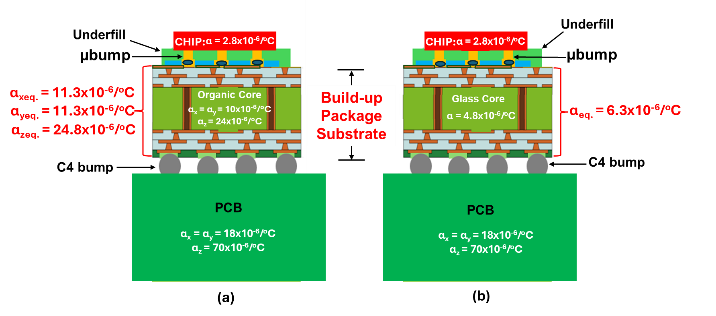
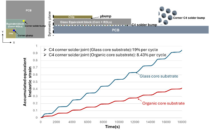
(3) Flip Chip with Microbump Interconnects
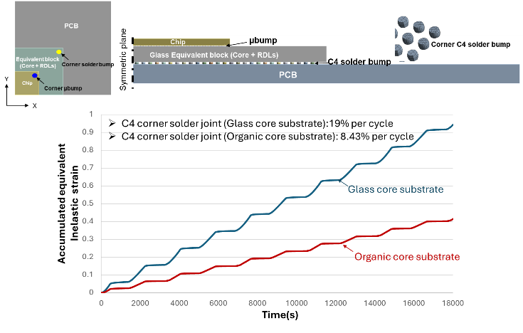
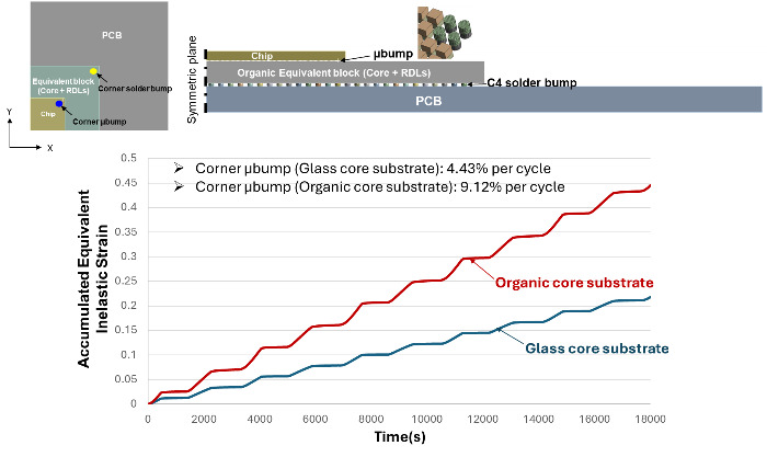
Figure 3 schematically shows the structures of Problem-One under consideration. From (Lau et al. 2025), we had shown that for the glass-core substrate, the accumulated equivalent inelastic strain in the µbump is 4.43% per cycle and in the solder joint is 19% per cycle (Figures 10 and 11). For the organic-core substrate, the accumulated equivalent inelastic strain in the µbump is 9.12 per cycle and in the solder joint is 8.43% per cycle. The temperature boundary condition is -45 ↔ 125oC.
(4) Flip Chip with Cu-Cu Hybrid Bonding
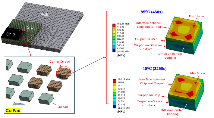
(4A) The Structure
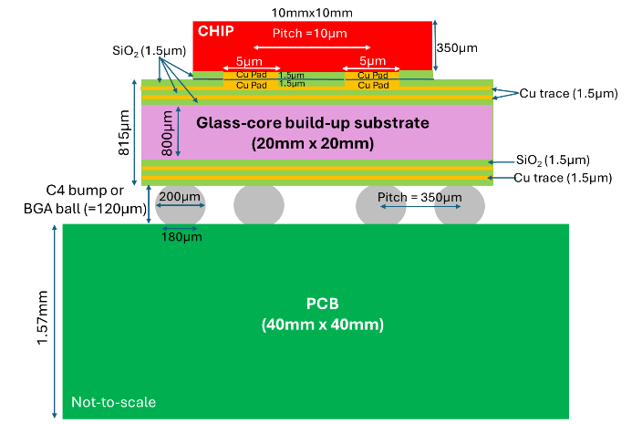
Figures and 12 schematically show the structure of Problem-Two under consideration. The silicon chip (10mm x 10mm x 350µm) with Cu-pad (5µm x 5µm x 1.5µm) is bonded to a glass-core build-up package substrate (20mm x 20mm x 815 Cu-Cu hybrid bonding. There are two build-up layers on the glass-core’s top and bottom sides which are fabricated by PECVD (plasma-enhanced chemical vapor deposition) for the SiO2 dielectric layer (1.5µm-thick) and Cu dual-damascene for the metal layer (1.5µm-thick). The Cu-pad pitch is 10µm. The geometry and material properties of C4 bump (solder ball) between the glass-core substrate and the PCB are the same as (Lau et al. 2025). It should be emphasized that unlike the organic-core substrate, the glass-core substrate is flat enough to perform Cu-Cu hybrid bonding.
(4B) Finite Element Modeling
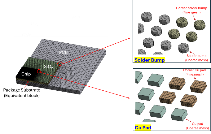
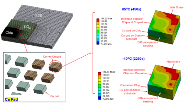
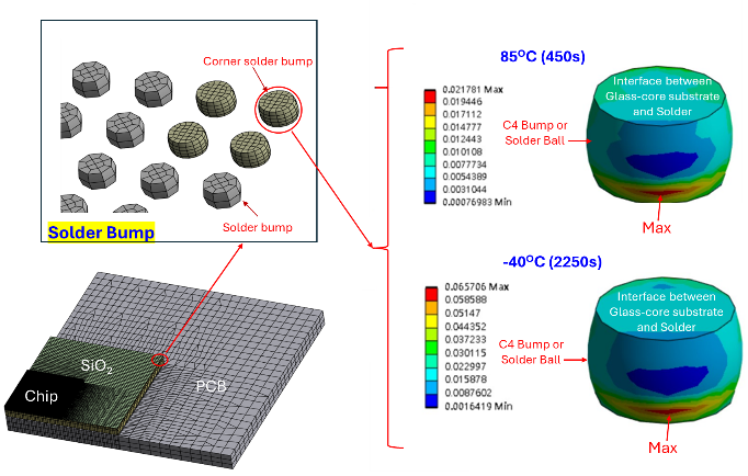
Figures 12 and 14 show the finite element models for the chip, package substrate, PCB (printed circuit board), Cu-Cu bonding interconnect, and C4 bumps. Finner meshes are used for the higher stress/strain areas such as corner Cu-Cu pads connecting the chip and the glass-core build-up package substrate and the corner C4 bumps (solder balls) connecting the build-up glass-core package substrate and the PCB.
.png)
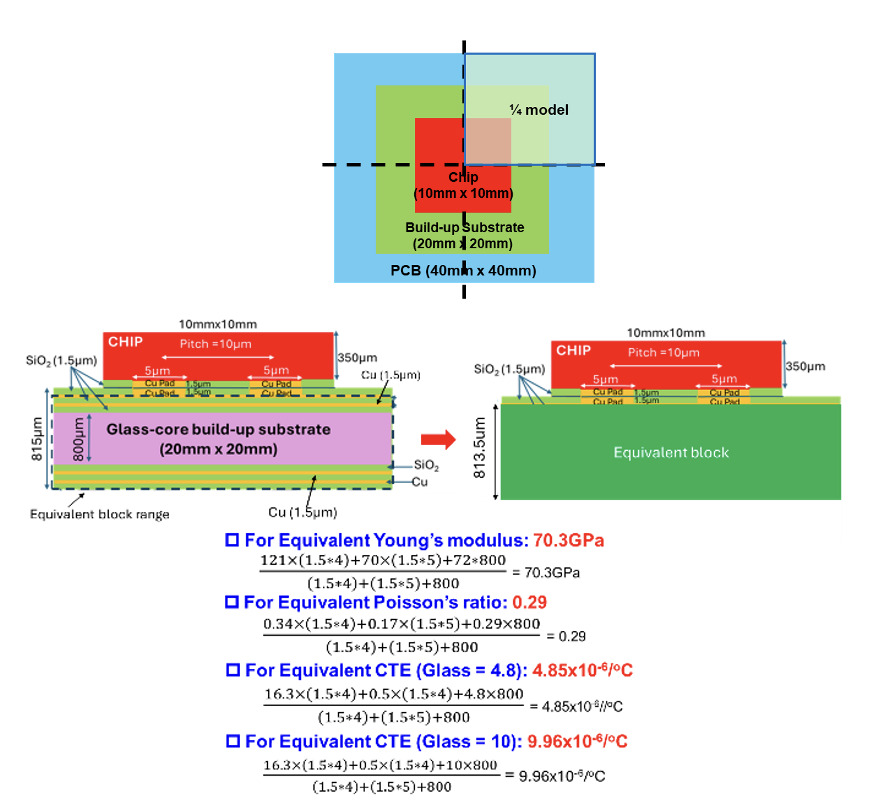
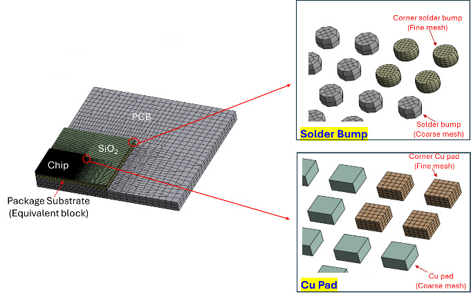
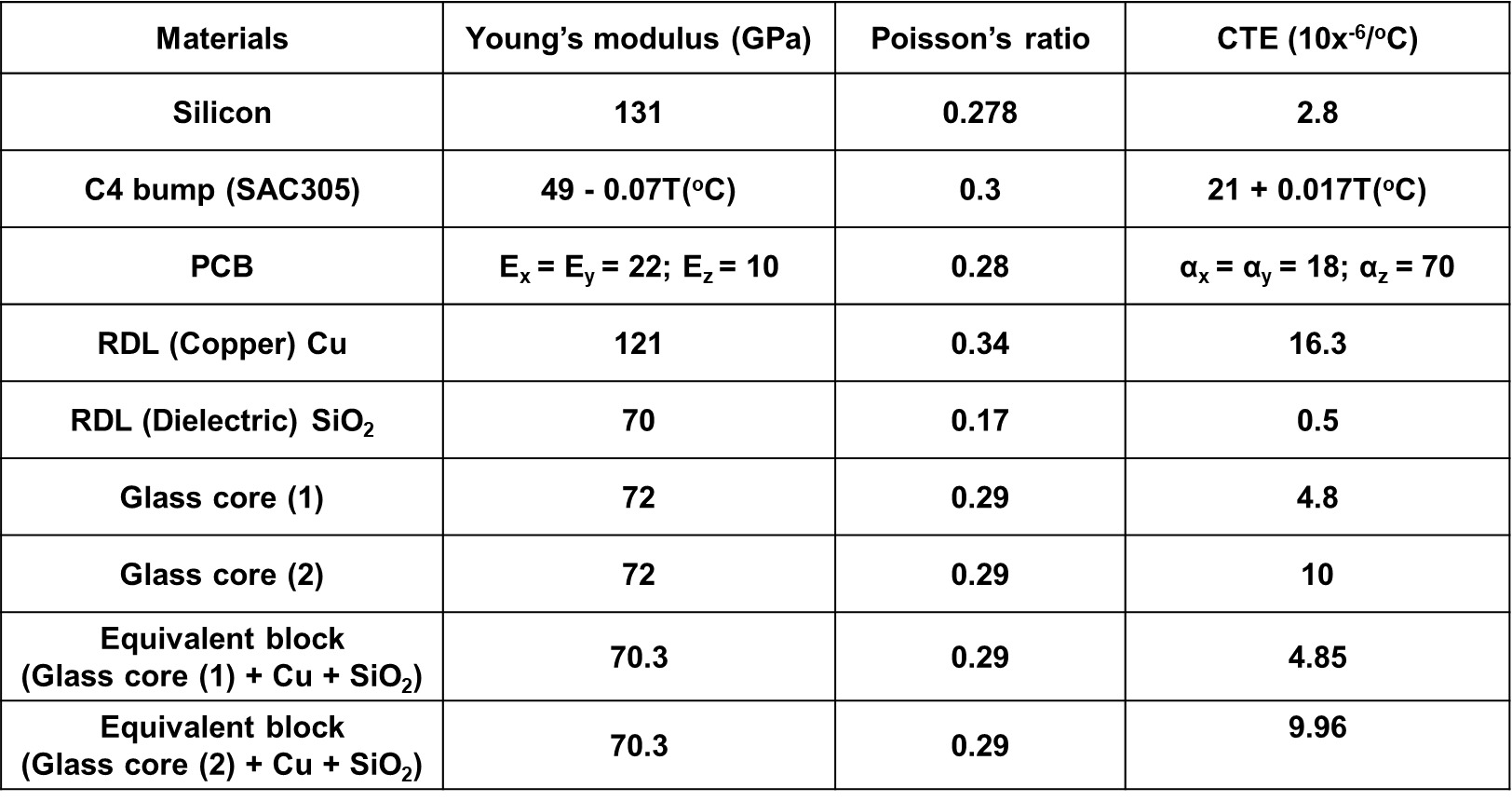
The glass-core substrate is modeled as an equivalent block as shown in Figure 12. The effective material properties of the equivalent block are shown in Table 1.
(4C) Materials Properties
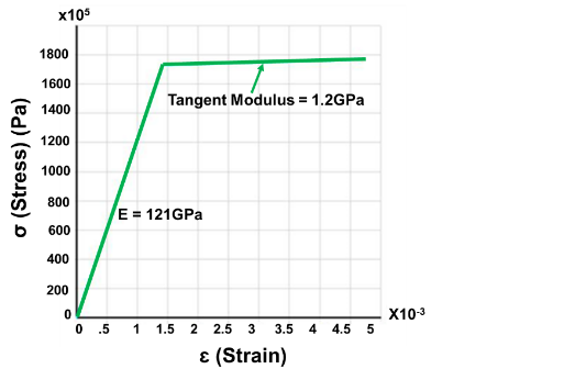
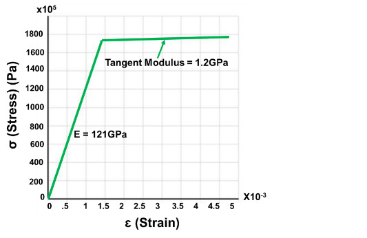
The effective material properties of the glass-core build-up equivalent block can be calculated by those shown in Figure 12 and are summarized in Table 1. The solder, Sn3Ag0.5Cu, obeys the Anand viscoplasticity constitutive equation (Chen et al. 2025) and the parameters of the Anand equation are shown in Table 2. The dual-damascene Cu is assumed to be an elastoplastic (bilinear kinematic hardening) material with the stress-strain relation shown in Figure 8 (first Young’s modulus = 121Gpa, second Young’s modulus = 1.2Gpa, and yield strength = 173MPa).
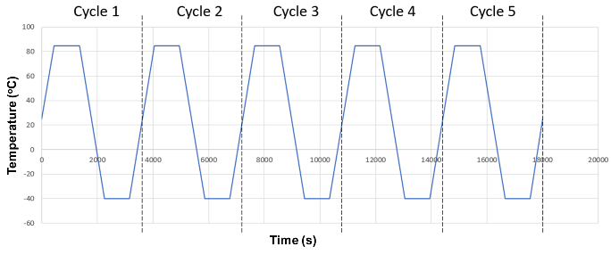
(4D) Temperature Boundary Condition
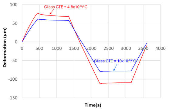
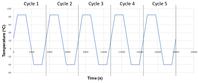
The temperature boundary condition is shown in Figure 15. Stress free is at room temperature (25oC).
(4E) Warpage of the Structure
The deformation of the flip chip bonded on the glass-core package substrate with Cu-Cu hybrid bonding and then solder balled on a PCB is shown in Figure 16. First of all, the deformation shapes are basically the same as those shown in Figure 6 of (Ostholt, Ambrosius, and Kruger 2014) (flip chip bonded on the glass-core package substrate with µbumps and then solder balled on a PCB). However, the deformation magnitudes of the structure with Cu-Cu hybrid bonding (84.35µm at 85oC (450s) and -119.45µm at -40 (2250s)) are larger than the structure with µbumps (73.22µm at 85oC (450s) and -103.48µm at -40 (2250s)). This could be due to the relaxation of the µbumps. (In this study, perfect diffusion Cu-Cu hybrid bonding [Lau and Fan 2025; Lau 2024a, 2025, 2024b, 2023, 2022] has been assumed). The time-history deformation of the structure with Cu-Cu hybrid bonding is shown in Figure 17. It can be seen that the deformation patterns are following the applied temperature boundary condition, Figure 15. The deformation of this size of chip is acceptable in most applications.


(4F) Accumulated Equivalent (von Mises) Stress
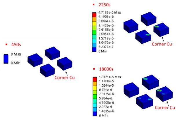
For flip chip solder interconnects, the focus is on the inelastic strain (Xing et al. 2025) while for flip chip Cu-Cu interconnects, the focus is on the stress. The strains in Cu-Cu perfect bonding are very small (in the 10-6 ranges) as shown in Figure 18.

_stress_contours_at_the_corner_cu-pads_at_450s_and_2250s.png)

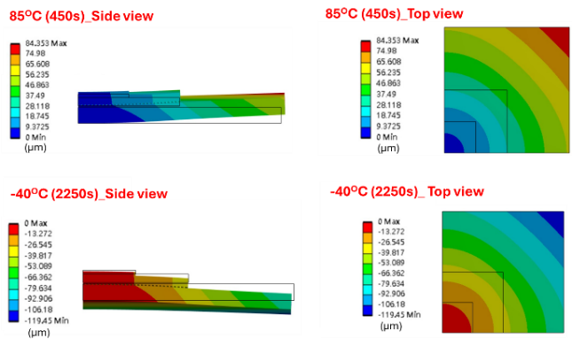
The Accumulated equivalent (von Mises) stress contours at the corner Cu-pads at 450s and 2250s are shown in Figure 19. The maximum stress location is at the interface between the Si chip and the Cu-pad. This is due to the large thermal expansion mismatch between the silicon (2.8x10⁻⁶/oC) and the Cu (16.3x10⁻⁶/oC) and stress concentration.
(4G) Accumulated Equivalent Inelastic Strain
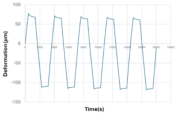
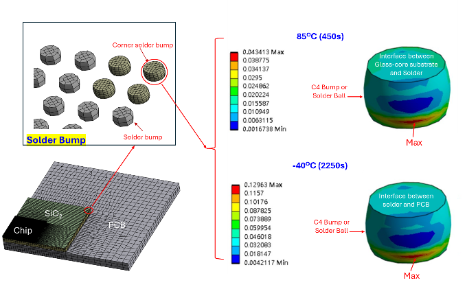
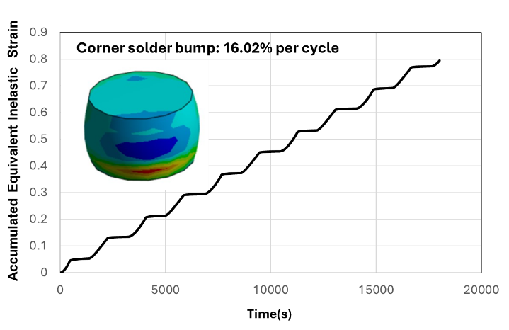
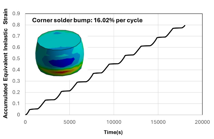
The accumulated equivalent inelastic strain contours at the corner solder ball at 450s and 2250s are shown in Figure 20. It can be seen that the maximum inelastic strain occurs near the interface between the solder ball and the PCB. This is due to the large thermal expansion mismatch between the glass-core (4.8x10⁻⁶/oC) and the PCB (18x10-6/oC). The time-history of accumulated equivalent inelastic strain is shown in Figure 21. It can be seen that the accumulated equivalent inelastic strain per cycle is 16.02%, which is quite high for the thermal fatigue life of the corner solder ball.
(4H) The CTE of Glass Increased from 4.8x10⁻⁶/oC to 10x10-6/oC
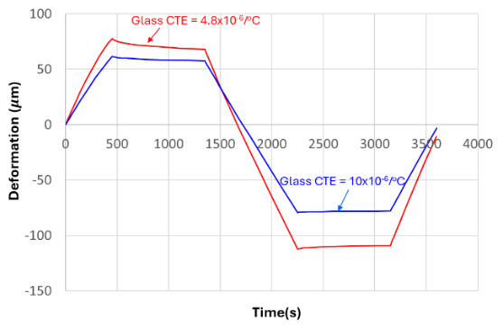
If the CTE of the glass core is increased from 4.8x10⁻⁶/oC to 10x10-6/oC (which is closer to the PCB) and subjected to the same temperature boundary condition (Figure 15), then the warpage, stress, and strain are shown in Figures 17-20. It can be seen from Figure 22 that the structure warpage for the CTE = 10x10-6/oC is slightly less than that for the CTE = 4.8x10⁻⁶/oC. Figure 23 shows the equivalent von Mises stress at the Cu-pad. It can be seen that the location of the maximum stress is the same as those with CTE = 4.8x10⁻⁶/oC and their magnitudes are basically the same. However, for the accumulated equivalent inelastic strain at the corner solder joint, the magnitudes are very different (Figure 24), and the strain is reduced from 16% per cycle to 8% per cycle (Figure 25). This is due to the reduction of the CTE of the glass core material, i.e., smaller thermal expansion mismatch between the glass core and the PCB.
.png)
.png)

(5) Summary
Based on simulation, some important results and recommendations are summarized as follows.
-
Just like the PCB, the organic-core build-up package substrate will be here to stay and used at huge volume for a long time. Glass-core build-up package substrate is able to seamlessly integrate optical interconnects, e.g. (Lau et al., n.d.), and will be used for niche applications, e.g., one-trillion transistors, e.g. (2023),.
-
For flip chip bonded to glass-core and organic-core substrates with µbumps.
-
For the µbump solder joint, the maximum accumulated equivalent inelastic strain is smaller in the structure with glass-core substrate than with organic-core substrate.
-
For the C4 solder joint, the maximum accumulated equivalent inelastic strain is more than two times larger in the structure with glass-core substrate than with organic-core substrate.
-
It is recommended that the CTE of the glass-core substrate should be closer to the CTE of
-
PCB (not to the CTE of Si chip) because there is no underfill protection of the C4 or BGA solder joints on the PCB, especially for larger glass-core substrates.
-
For flip chip bonded to glass-core substrate with Cu-Cu hybrid bonding.
-
Unlike organic-core substrates, the glass-core substrates are flat enough to perform Cu-Cu hybrid bonding.
-
For extremely fine-pitch, high-density, and high-performance applications, the L/S of the RDLs of the glass-core substrate are usually less than 2µm. The dielectric layer (SiO2) can be fabricated by PECVD and the metal layer by dual-damascene Cu + CMP (chemical-mechanical polishing).
-
The warpage of the flip chip bonded on glass-core substrate with Cu-Cu hybrid bonding are very similar to that of the flip chip bonded on glass-core substrate with µbumps, except the magnitudes. The magnitudes of the Cu-Cu hybrid bonding are larger than those of the µbumps. This is because of the relaxation of the µbumps.
-
The maximum accumulated equivalent inelastic strains in Cu-Cu hybrid bonding are very small.
-
The maximum accumulated equivalent (von Mises) stress occurs at the interface between the Si chip and the Cu-pad.
-
The maximum accumulated equivalent inelastic strain occurs near at the interface between the solder ball and the PCB.
-
The accumulated equivalent inelastic strain per cycle is 16.02%, which is smaller than that with µbump (19%). However, it is still quite high for the solder joint reliability. A larger CTE for the glass-core substrate is recommended.
-
By increasing the CTE of glass core from 4.8x10⁻⁶/oC to 10x10-6/oC, the warpage of the structure reduced by 48% and the accumulated equivalent inelastic strain reduced by 50%.