


1. Introduction
Co-packaged optics (CPO) are heterogeneous packaging methods to integrate the chiplets such as the optical engine (OE), which consists of PICs and the electrical engine (EE), which consists of EICs as well as the switch application-specific IC (ASIC). The advantages of CPO are (a) Reducing the length of the electrical interface between the OE/EE (or PIC/ EIC) and the ASIC; (b) Reducing the energy required to drive the signal; and (c) Cutting the latency, which leads to better electrical performance (Takemura et al. 2022; Ackermann et al. 2022; Lee et al. 2023; Lars Brusberg et al. 2022; Noriki et al. 2023; L. Brusberg et al. 2022; Tan et al. 2023; Grenier et al. 2023; Yoshida et al. 2025; L. Brusberg et al. 2025; Knickerbocker et al. 2025; Lo et al. 2025; Singh et al. 2025; M. F. Chen et al. 2025; Mehta et al. 2025; Noriki et al. 2025; Lin et al. 2024; Deo et al. 2024; L. Brusberg et al. 2024; Mizuno et al. 2024; Umeta et al. 2024; Steenberge et al. 2024; Nakamura et al. 2024; Noriki and Amano 2023; Yeary et al. 2023; Gupta et al. 2023; Bhuvanendran et al. 2023; Li et al. 2023; McDonough et al. 2023; “Integrated Optical Interconnect Systems (iOIS) for Silicon Photonics Applications in HPC,” n.d.; Hsia et al. 2023; Lu et al. 2022; Application Chou et al. 2022; Razdan et al. 2022; Janta-Polczynski and Robitaille 2022; Maharry et al. 2021; Nieweglowski et al. 2020; Johnson et al. 2022; Lau 2022, 2024a, 2023c; Lau and Tseng 2024, 2025; Lau et al., n.d.).
Twenty years ago, silicon integration was very popular. Companies like Intel have been promoting silicon photonics which integrate some of the PIC, EIC, and waveguides on a chip from a silicon wafer with complementary metal-oxide semiconductor (CMOS) technology. The holy grail of silicon photonic is to integrate all the PIC and EIC on a chip fabricated from a Si wafer with CMOS technology. However, in the past few years, driven by cost, the PIC and EIC are partitioned and split into small chiplets (Lau and Fan 2025; Lau 2024b, 2023a, 2021, 2019) and then integrated on a substrate. The key advantages of silicon photonics are better performance and easier to test. The key disadvantages of silicon photonics are higher costs and more rigid infrastructure. The key advantages of chiplets are lower costs and more flexible. The key disadvantages of chiplets are not as good performance as silicon photonics and larger package size. This study is focused on the heterogeneous integration of the chiplets such as the ASIC switch, PIC, EIC, and silicon photonics of the silicon integration of the PICs and EICs.
2. Photonic Devices and Silicon Photonics
Photonic devices are components that generate, manipulate, and detect light, e.g., LED (light emitting diode), lasers, photodiode (PD), etc.
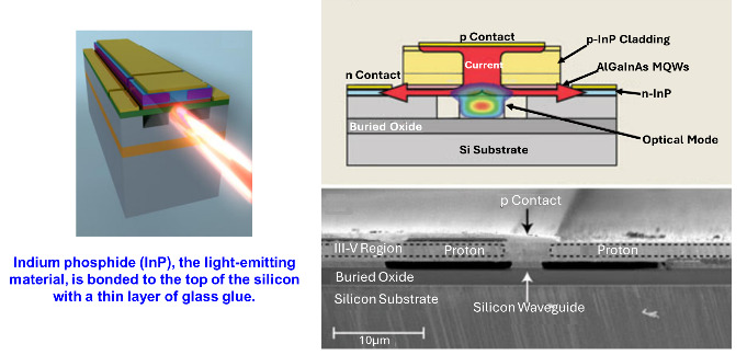
Silicon photonics is a technology that integrates optical components onto a silicon chip, enabling the transmission of data using light instead of traditional electrical signals. In another words, silicon photonics are the semiconductor integration of some of the PIC, EIC, and waveguides on a silicon wafer with CMOS technology. As shown in Figure 1, after the IC is fabricated on the silicon wafer, the indium phosphide (InP; a light-emitting material) is bonded to the top of the silicon wafer with a thin layer of glass glue. This is what Intel called the hybrid laser technology, in which the IC and laser are manufactured by the CMOS technology on the same silicon wafer. Some of the advantages include the automation of on-wafer optical, electrical, and high speed test and wafer-level burn-in.


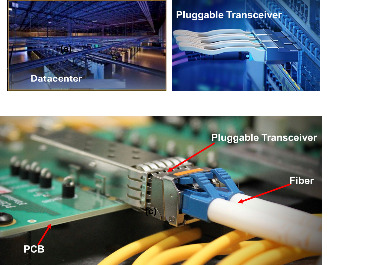
3. Data Centers
A data center includes switches, routers, storage solutions, etc., such as those shown in Figure 2. Their functions include the network of computing and storage resources that enable the delivery of shared applications and data. Today, more than 90% of transceivers are pluggable transceivers (Lau, Erasmus, Sporon-Fiedler, Murphy, et al. 2001; Lau, Erasmus, Sporon-Fiedler, and Chang 2001; Lau, Jiaa, and Erasmus 2001; Lau et al. 2002). Figure 3 shows the future optical transceivers on a common package substrate (CPO) used in a data center.

4. Optical Transceivers
Optical transceivers are the most important component in a data center. An optical transceiver is a key component of an optical transmission system that permits coupling of the transmission medium with the active components of the chain, such as switches, routers, optical interfaces or any optical transport equipment. An optical transceiver defines the process of converting electric signaling toward the optical transmission with the help of the transmission optical subassembly (TOSA), or Tx module and performing inverse action through the receiver optical subassembly (ROSA), or Rx module (Figure 3). A TOSA contains a semiconductor laser diode (LD), laser driver, etc., while a ROSA contains a photodiode (PD), an optical interface such as a lens, a transimpedance amplifier (TIA), a passive electrical interface, etc. The TOSA module converts the electrical signal to the optical transmission light that lands on the fiber. The ROSA is used to receive an optical signal from a fiber and convert it back into an electrical signal.


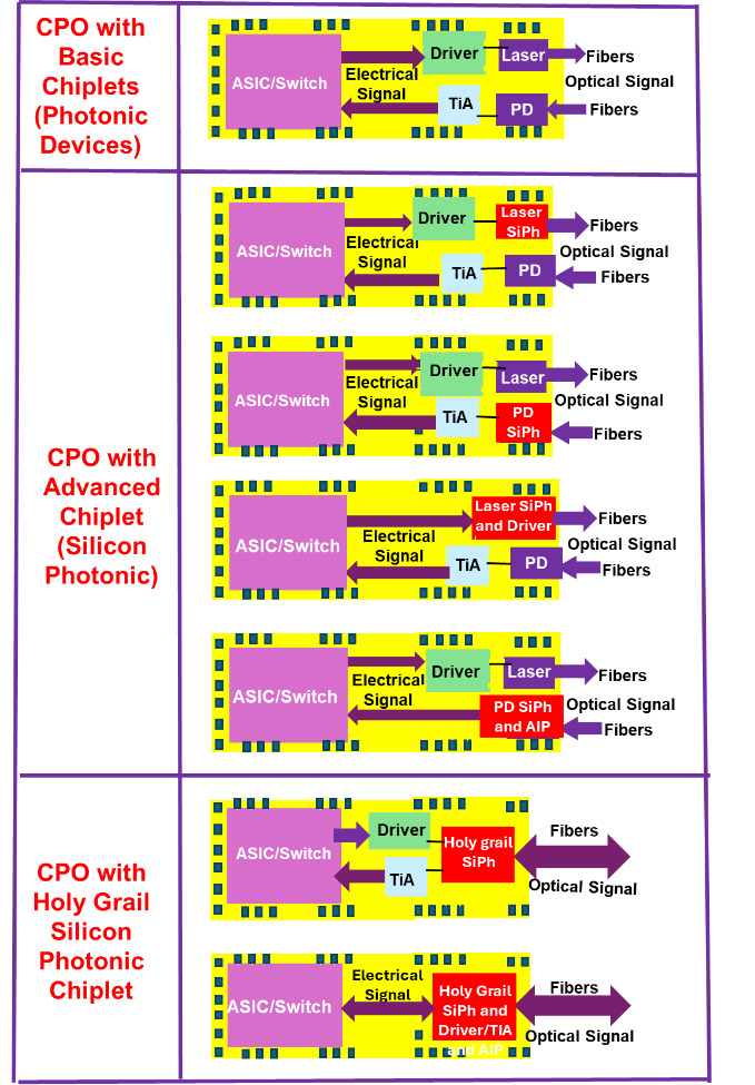
There are many forms of transceivers in CPO as shown in Figure 4. The most common form is the CPO with the basic chiplets such as switch, laser driver, TIA, and the photonic devices such as the laser, and PD. The advantages are lower cost and more flexibility. The disadvantages are larger package size and more work in testing and burn-in. The next common form is the CPO with advanced chiplets such as the silicon photonic laser chip, silicon photonic PD chip, silicon photonic laser and driver chip, silicon photonic PD and TIA chip, etc. The advantages are better performance, easier to test and burn-in, and smaller package size. The disadvantages are higher costs and more rigid infrastructure. The CPO with the holy grail silicon photonic chip which integrates all the PIC such as the laser and PD and even all the EIC such as the driver and TIA from a silicon wafer with CMOS technology is nowhere in sight.
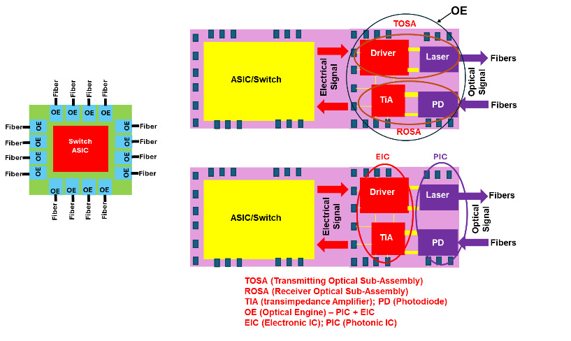
5. Optical Engine and Electrical Engine
The OE and EE are the key components of the optical transceiver for realizing photoelectric signal conversion. For example, the OE of an optical transceiver consists of the PIC, such as the PD and laser, etc., as shown in Figures 3 and 4. On the other hand, the EE of an optical transceiver consists of the EIC such as the laser driver and TIA, etc. Sometimes, OE is used to represent the OE + EE.
6. Pluggable Optics, On-Board Optics, Near-Package Optics, and Co-Packaged Optics
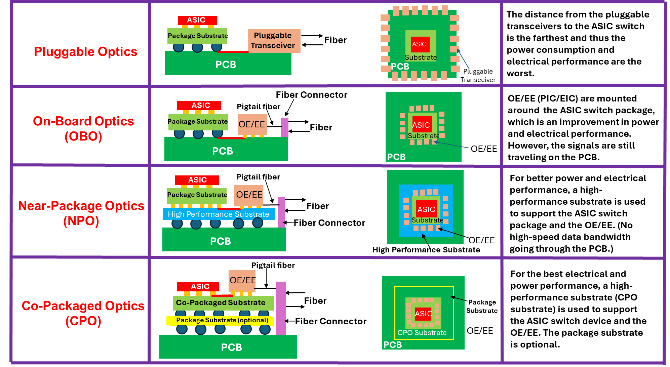
The pluggable optics, OBO, NPO, and CPO are schematically summarized in Figure 5. It can be seen that the pluggable transceivers are mounted on the edges of a printed circuit board (PCB) with the ASIC package attached to a package substrate. The distance from the PIC/EIC of the pluggable transceivers to the ASIC chip is the farthest and therefore, the power consumption and electrical performance are the worst.
Since 2018, the key components such as OE and EE (PIC/EIC) of the transceivers have been mounted on the same PCB as the packaged ASIC and arranged on the four sides of the packaged ASIC. This scheme is called OBO (on-board optics), which uses the PCB to perform the connection between the packaged ASIC and the OE/EE. The distance between the PIC/EIC and the ASIC is closer than the pluggable optics and therefore, there is an improvement in power and electrical performance.
Since 2020, some people placed the OE/EE side-by-side with the packaged ASIC on the same high-performance substrate. This is called NPO (near-package optics) and uses the high-performance substrate to perform the connection between the packaged ASIC and the OE/EE. There is no high-speed data bandwidth going through the PCB, so better power and electrical performance can be achieved. According to the Optical Internetworking Forum (OIF) - for NPO applications - lengths between the ASIC and optics can be up to 150mm with the channel loss constrained to 13dB. This is why the OIF is developing the extra short reach (XSR) + electrical interface, to expand the XSR’s reach for NPO.
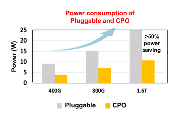
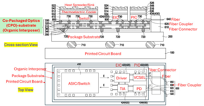
Since 2023, after the shipment of CPO by Intel and Broadcom, people are very interested in CPO. In CPO, the OE/EE is placed side-by-side along the four edges of the ASIC chip on the same co-packaged substrate. In this case, the distance between the ASIC and the PIC/EIC is the shortest and therefore has the best electrical performance. In short, NPO brings the PIC/EIC closer to the ASIC package on a high-performance substrate, while CPO brings the PIC/ EIC and the ASIC chip side-by-side on the same co-packaged substrate. CPO offers superior formfactor, power consumption, and latency benefits compared to NPO. According to OIF, CPO confines the modules OE/EE and host ASIC chip to be within 50mm of each other. The channel loss here is limited to 10dB. CPO has a lower power consumption, Figure 6 (Johnson et al. 2022), because of the shorter spans and 3dB saving.


7. CPO Substrates
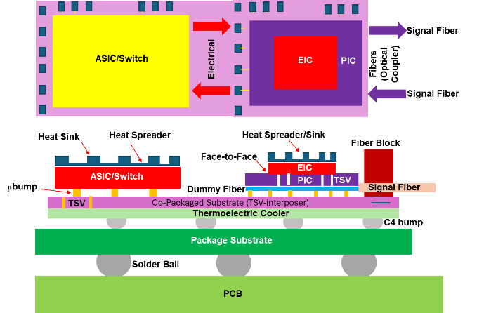
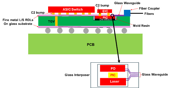
There are many different types of CPO substrates such as silicon, Figure 7 (Lau 2022, 2024a), glass, Figure 8 (Lau 2024a), and organic, Figure 9 (Lau and Tseng 2024), etc. Silicon substrates such as the through-silicon via (TSV)-interposer have been presented in great detail in, e.g (Lau 2016, 2013). Glass substrates such as the laser-induced deep etching (LIDE) process developed by LPKF Laser & Electronics AG in 2017 has been reported in (Lau 2025b; Xing et al. 2025; L. Chen et al. 2025; Sunohara et al. 2025). Figure 9 shows a 2D heterogeneous integration of ASIC, EIC and PIC on a CPO organic interposer (Lau and Tseng 2024). It can be seen that the ASIC switch chip, EIC chips and PIC chips are side-by-side attached to the CPO organic interposer with µbumps.
_cpo_on_an_organic-core_or_a_glass-core_package_substrate._(b)_cpo_on_a_tsv__a_tgv__or_a.png)
_cpo_with_emib_embedded_in_an_organic_build-up_package_substrate._(b)_cpo_with_si_bridge.png)

8. Heterogeneous Integration of Switch, PIC and EIC
8.1. 2D Heterogeneous Integration of ASIC Switch, PIC and EIC
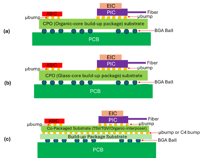
Figure 10(a) shows a 2D COP system. It can be seen that the ASIC switch, PIC, and EIC are side-by-side attached on a CPO substrate, which can be an organic-core build-up package substrate or a glass-core build-up package substrate. Figure 10(b) shows another CPO system. It can be seen that the switch, PIC, and EIC are side-by-side attached to a CPO substrate which can be either a TSV-interposer, a TGV-interposer, or an organic-interposer. The interposer is then attached to an organic build-up package substrate.
The CPO system shown in Figure 10(b) is for higher performance applications than that of Figure 10(a), but with higher cost.

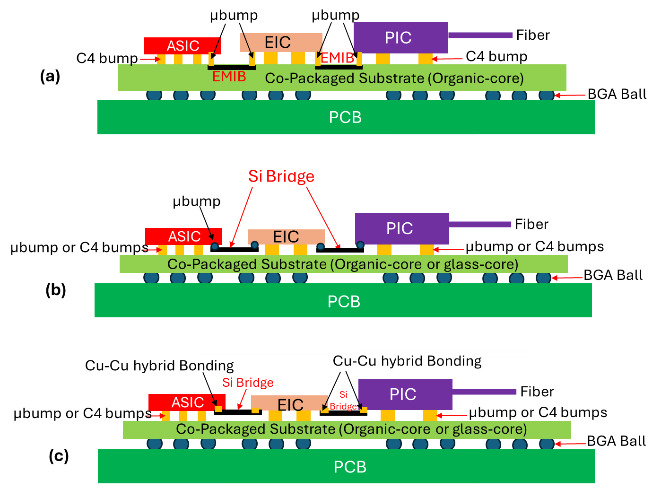
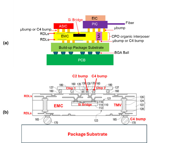
8.2. 2D Heterogeneous Integration of ASIC Switch, PIC and EIC with Si Bridges
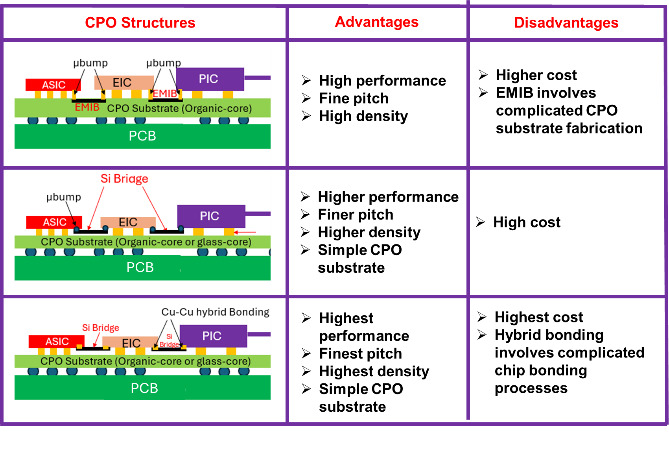
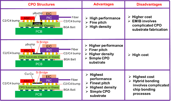
Figure 11(a) shows a CPO system. It can be seen that the chiplets such as the switch, PIC, and EIC are side-by-side attached to an organic build-up package substrate with embedded multi-die interconnect bridge (EMIB) (Mahajan et al. 2016) connecting the switch and EIC and the EIC and PIC. Figure 11(b) shows another CPO system. It can be seen that the switch, PIC, and EIC are side-by-side attached to either an organic-core substrate or a glass-core substrate. The Si bridge is connected between the switch and the EIC and the EIC and the PIC with microbumps. It is noted that the Si bridges are not embedded in the CPO organic-core or glass-core build-up package substrate. Figure 11(c) shows another CPO structure. It can be seen that the switch, PIC, and EIC are side-by-side attached to either a glass-core substrate or an organic-core substrate. The Si bridge is connected between the switch and the EIC and the EIC and the PIC with Cu-Cu hybrid bonding. A comparison of these three CPO structures is shown in Figure 12.
8.3. 3D Heterogeneous Integration of ASIC Switch, PIC and EIC
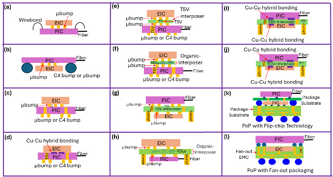
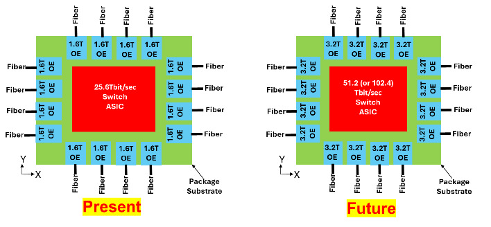
With CPO, the switch chip is typically surrounded by 16 OEs, all placed on a package substrate. Currently, the 25.6-terabit Ethernet switch chip (Figure 13a) requires 16@1.6 terabits-per-second (1.6Tbps) OEs, while the upcoming 51.2-terabit switch chips (Figure 22b) will use 3.2Tbps OEs (the size of the EIC and PIC of the OE will be larger). The issue is that the multi-chip module can only be so large. It is challenging with today’s packaging technology to surround the 51.2Tbps ASIC with 16@3.2Tbps (or 102.4Tbps ASIC with <16@6.2Tbps>) OEs. One of the solutions is to integrate some of the PIC and EIC into a silicon photonic by CMOS technology and then attach the silicon photonic to a CPO substrate. Another solution is to stack up the PIC and the EIC (from 2D to 3D) with heterogeneous integration packaging method.
There are many different kinds of 3D heterogeneous integration (stacking) of the PIC and EIC as shown in Figure 14. It can be seen from Figure 14a that the light is coming from the fiber to the PIC and the PIC and EIC are stacked (face-to-face) with the µbumps, and the signals are fanning out through the wire bonds from the PIC. Figure 14b is basically the same as Figure 14a except the signals are fanning out through the C4 bumps, or µbumps, from the PIC. Figure 14c shows the EIC and the PIC are stacked (face-to back) with the µbumps, and the signals are running out through the TSVs and the C4 bumps or µbumps from the PIC. Figure 14d is basically the same as Figure 14c except the µbumps between the EIC and PIC are eliminated by the bumpless Cu-Cu hybrid bonding. Figure 14e shows that the EIC and the PIC are stacked (connected) by a TSV-interposer with the µbumps, and the signals are fanning out through the RDLs and TSVs of the TSV-interposer and the TSVs and C4 bumps or µbumps from the PIC. Figure 14f is basically the same as Figure 14e except the TSV-interposer is replaced by the organic-interposer and the signals are fanning out through the RDLs of the organic-interposer and the TSVs and C4 bumps or µbumps from the PIC. Figure 14g shows that the PIC and EIC are stacked by a TSV interposer with µbumps, and the signals are running out through the µbumps of the TSV-interposer. Figure 14h is basically the same as Figure 14g except the TSV-interposer is replaced by the organic-interposer. Figure 14i is basically the same as Figure 14g except the µbumps on both sides of the TSV-interposer have been eliminated by the bumpless Cu-Cu hybrid bonding. Figure 14(j) is basically the same as Figure 14(i), except the TSV-interposer is replaced by the TGV-interposer.
Comparing Figure 14c with Figures 4.23e and 4.23f, the latter figure represents the case for extremely high-density situations and the case where there are difficulties in direct stacking of the EIC and PIC. Comparing Figure 14e with Figure 14g, it can be seen that the TSVs in the PIC as shown in Figure 14e have been eliminated (see Figure 14g). Similarly, by comparing Figure 14f with Figure 14h, it can be seen that the TSVs in the PIC - as shown in Figure 14f - have been eliminated (see Figure 14h).


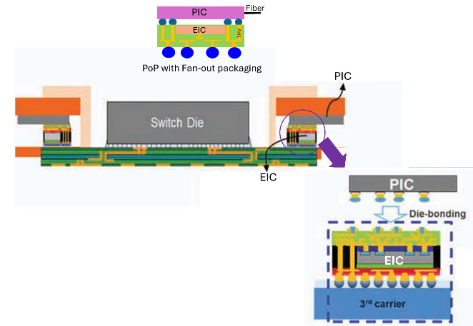
Figures 14k and 14l are package-on package (PoP) of the PIC and EIC. Figure 14k is for a solder-bumped flip-chip application for the EIC on a package substrate, while Figure 14l is for the fan out of the EIC on a set of RDLs.
_3d_cpo_on_organic-core_package_substrate._(b)_3d_cpo_on_glass-core_package_substrate._(.png)
_3d_cpo_with_microbumped_emib_embedded_in_an_organic_build-up_package_substrate._(b)_3d_.png)
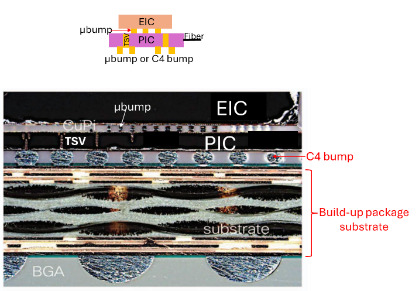
The patent application of case (h) has been granted (Lau and Tseng 2024) and is shown in Figure 15. It can be seen that the EIC and PIC are stacked with an organic interposer and the CPO substrate for the 3D heterogeneous integration of the PIC and EIC as well as the switch is a build-up package substrate. Figure 16 shows a CPO system with EIC stacked on top of PIC with TSVs (Razdan et al. 2022), which is case (c) of Figure 14. Figure 17 shows a CPO system with POP structure (Lin et al. 2024). It can be seen that the PIC is stacked on top of the EIC which is embedded in the fan-out EMC, case (l) of Figure 14.
Figure 18(a) shows a 3D heterogeneous integration (stacking) of PIC and EIC (such as those shown in Figure 14) side-by-side with the ASIC switch with µbumps or C4 bumps on a CPO organic-core build-up package substrate. Figure 18(b) shows a 3D heterogeneous integration of PIC and EIC side-by side with the ASIC switch on a same CPO glass-core build-up package substrate. Figure 18(c) shows a 3D heterogeneous integration of PIC and EIC side-by side with the ASIC switch on a same CPO TSV/TGV/organic-interposer. Then, the interposer is attached to an organic build-up package substrate. The CPO system shown in Figure 18(c) has the highest performance and cost. The CPO system shown in Figure 18(a) has the lowest performance and cost.


8.4. Heterogeneous Integration of ASIC Switch, PIC and EIC with Bridges
Figure 19(a) shows a 3D heterogeneous integration of PIC and EIC (such as those shown in Figure 14), as well as the ASIC switch with Intel’s embedded multi-die interconnect bridge (EMIB) in the cavity of a CPO organic-core package substrate. The bridge is connecting the switch and the PIC. There are two different kinds of bumps (µbumps and C4 bumps) on the ASIC and PIC. Figure 20 shows one of Intel’s CPO systems with their EMIB (Singh et al. 2025).
Figure 19(b) shows a 3D heterogeneous integration of PIC and EIC, and an ASIC with silicon bridges. It can be seen that the ASIC and the 3D stacking of EIC and PIC are connected with a silicon bridge with µbumps. Then, the ASIC and the 3D stacking of EIC and PIC are attached to a CPO organic-core substrate or glass-core substrate with either µbumps or C4 bumps. The bridge is not embedded in the substrate. An example of Si bridge connecting two chiplets is shown in Figure 21 for Apple’s notebook computers shipped in 2022.
_cop_on_fan-out_emc_with_embedded_si_bridge._(b)_si_bridge_embedded_in_fan-out_emc_with_.png)

Figure 19(c) shows a 3D heterogeneous integration of PIC and EIC, and an ASIC with a silicon bridge, which is exactly the same as Figure 19(b) except the connection between the switch (or PIC) and the bridge is with Cu-Cu hybrid bonding. Apple shipped their notebook with Cu-Cu hybrid bonding between the chiplets (CPU and GPU) and the Si bridge in Q4 2025. A comparison between these three cases is shown in Figure 19.
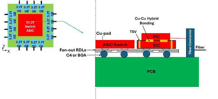
8.5. 3D Heterogeneous Integration of PIC, EIC, and ASIC Switch on Fan-out RDL substrate
Figure 22(a) shows a CPO system. It can be seen that the PIC and EIC are stacked with Cu-Cu hybrid bonding and then they are side-by-side with a switch attached to a fan-out with RDLs CPO substrate. The CPO substrate is then attached to a PCB. The structure is very simple with high performance and reasonable cost. Figure 22(b) shows a similar patent (Lau et al. 2022).
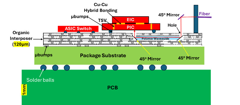
8.6. 3D Heterogeneous Integration of PIC, EIC, and ASIC Switch on Fan-out RDLs and Polymer Waveguides
Figure 23 shows a CPO system. It can be seen that the PIC and EIC are 3D stacked with hybrid bonding and then they are side-by-side with a switch attached to a fan-out RDLs CPO substrate. Figure 24 shows another CPO system. It can be seen that the PIC and EIC are 3D stacked with hybrid bonding and then they are side-by-side with a switch attached to a fan-out RDLs CPO substrate with holes. The holes are used for lights to pass through. There are polymer waveguides with 45° mirrors at their both ends semi-embedded in the PCB. The light from the external fiber through the V- groove hits the 45° physical mirror and then reflects and passes through the hole and hits one end of the
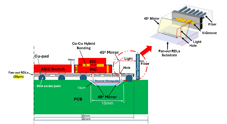

mirror of the polymer waveguide. The light travels along the polymer waveguide, hits the other end of the 45° mirror, and then reflects on the PIC. Finally, the PD of the PIC receives the light. This system has better performance than that shown in Figure 23 but with higher cost.
8.7. 3D Heterogeneous Integration of EIC, PIC, and ASIC Switch on Embedded Polymer Waveguide and Organic Interposer
Figure 25 shows another CPO system. It can be seen that the PIC and EIC are stacked with hybrid bonding and then they are side-by-side with the switch attached to an organic interposer with an embedded polymer waveguide with 45° mirrors at its both ends. There are holes in the organic interposer. The CPO interposer is attached to a build-up package substrate and then on a PCB. Compared with the CPO systems shown in Figures 23 and 24, this system has the best performance but has the highest cost.


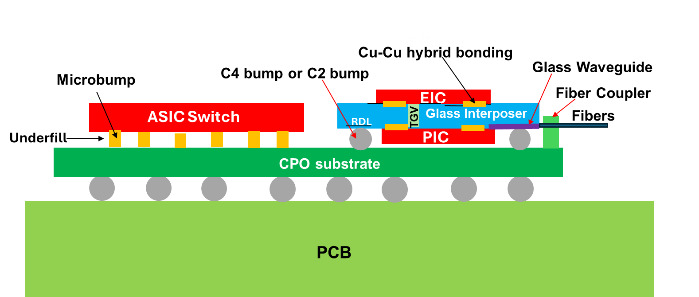
8.8. 3D Heterogeneous Integration of ASIC, PIC, and EIC with Glass Interposer
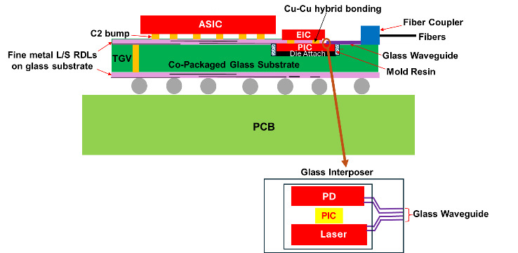
Figure 26 shows a CPO system with TGV-interposer. It can be seen that the PIC and EIC are 3D stacked through a TGV-interposer with Cu-Cu hybrid bonding. The PIC and EIC are side-by-side with the switch attached to a build-up package substrate. Then, the package substrate is attached to the PCB. The glass waveguide on the glass interposer receives the light from the external fiber and sends the light to the PD of the PIC.
8.9. 3D Heterogeneous Integration of ASIC, PIC and EIC with Glass Substrate
Figure 27 shows a CPO structure with a glass-core build-up package substrate. It can be seen that there is a cavity on the CPO glass-core substrate. The PIC and EIC are 3D stacked with hybrid bonding and the PIC is semi-embedded in the cavity of the substrate. The switch and the PIC/EIC stack are side-by-side attached to the CPO substrate. Compared to the CPO structure shown in Figure 26, this CPO structure has better performance but has higher cost.
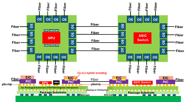
9. 3D CPO for HPC Driven by AI and High-Speed and High-Bandwidth Communications

Figure 28 shows a CPO system for HPC driven by AI and high-speed and high-bandwidth communication applications. It can be seen that the graphics processing unit (GPU) is surrounded by the high-bandwidth memory (HBM) and then surrounded by the OE such as the PIC and EIC. The ASIC switch is surrounded by the PIC and EIC. For both structures, the PIC and EIC are 3D stacked by Cu-Cu hybrid bonding. The GPU, HBM, and the stacking of the EIC and PIC are side-by-side on the same co-packaged substrate, which can be a TSV-interposer, TGV-interposer, or organic-interposer. Similar to the ASIC switch and PIC/EIC. These two structures are then attached to a PCB.
10. Summary and Recommendations
Some important results and recommendations are summarized in the following.
-
Photonic devices are components that generate, manipulate, and detect light, e.g., LED (light emitting diode), lasers, photodiode, etc.
-
Silicon photonics is the integration of some or all of the PIC and EIC into a 2D chip from a silicon wafer with CMOS technology.
-
Twenty years ago, silicon integration was very popular. Companies like Intel have been promoting silicon photonics. The holy grail of silicon photonic is to integrate all of the PIC and EIC into a single 2D chip fabricated from a silicon wafer with CMOS technology.
-
However, in the past few years, driven by cost, the PIC and EIC are partitioned and split into small chiplets.
-
CPO is the heterogeneous integration packaging method to integrate all the chiplets such as the switch, PIC, EIC, and silicon photonic on a CPO substrate or interposer.
-
Various forms of CPO have been shown in Figure 4, where their advantages and disadvantages have been given. CPO with basic chiplets will be used the most. CPO with advanced chiplet (silicon photonic) will be used less. CPO with the holy grail silicon photonic is nowhere in sight.
-
Various systems (structures) of CPO with Si bridges have been shown in Figure 12, where their advantages and disadvantages have been given.
-
Twelve different 3D stacks of PIC and EIC have been given in Figure 14 and some of their advantages and disadvantages have also been briefly mentioned.
-
Various new structures (systems) of CPO have been proposed. Their substrate can be fan-out RDLs, fan-out RDLs with holes and polymer waveguides in the PCB, an organic interposer with holes and embedded polymer waveguides, a TGV interposer, a glass-core build-up package substrate, etc.
-
Figure 28 shows a future CPO system for HPC driven by AI and high-speed and high-bandwidth communications.
-
As of today, there is not any paper published in the quality and reliability (such as the thermal-cycling, thermal shock, mechanical vibration, mechanical shock, high-temperature storage, highly accelerated temperature, highly accelerated moisture resistance etc.) of CPO. In order for CPO to be more popular, these quality and reliability data are desperately needed. Thermal management of 3D CPO will be an important topic.
-
More use of the glass substrate or glass interposer for CPO.
-
Just like electrical leakage, light leakage due to coupling loss, waveguide cracks, scattering, and absorption can all become invisible killers and should also be noted.
-
Due to the requirement of higher interconnect density, finer pitch, more compact 3D integration, lower power consumption, lower latency, higher bandwidth, and better signal integrity of a CPO system, the Cu-Cu hybrid bonding (Lau 2022, 2026, 2025a, 2024c, 2023b) of some of the PIC and EIC are strongly recommended.