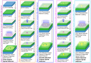
_computer-aided_design_(cad)_mask_created_using_clewin_software_for_laser_direct_writin.tiff)
_optical_microscope_image_.tif)
I. Introduction
The rapid growth of high-performance computing (HPC), fifth-generation (5G) wireless, and miniaturized electronics have intensified the demand for compact, high-Q passive components—particularly embedded inductors. These components are essential for on-chip power management, radio frequency (RF) communication, signal processing, and local energy storage. As integrated circuits (ICs) and system-on-chip (SoC) platforms continue to shrink in lateral dimensions while incorporating increasingly complex functionalities, designers are now targeting inductance densities above ≈50 nH/mm² and quality factors (Q) exceeding 30 at 1 GHz—all within footprints of just a few square millimeters. To meet these performance goals, embedded inductors are increasingly implemented in multilayer (multi-stacked) configurations to boost inductance within constrained footprints (Zolfaghari et al. 2003). However, fabricating such structures poses significant challenges, as inductance is highly dependent on the inductor’s geometry and the effective length of the magnetic flux path. Achieving miniaturization often necessitates multilayer stacking, the use of high-conductivity materials, and precise vertical interconnection; requirements that conventional fabrication methods struggle to fulfill reliably (Banerjee 2023).
Each of the conventional approaches—subtractive, additive, and hybrid—faces inherent limitations that constrain their suitability for advanced miniaturized fabrication (Iqbal et al. 2020). Subtractive methods involve complex, multi-step workflows with significant material waste and limited compatibility with flexible or biodegradable substrates. Additive techniques, while more sustainable, often do not provide the resolution and alignment accuracy required for vertical stacking. Hybrid subtractive–additive methods aim to combine the strengths of both approaches, but they often introduce greater process complexity and limited scalability due to extended processing times and alignment challenges (Grzesik and Ruszaj 2021).
These persistent limitations underscore the urgent need for a new fabrication approach that is fully additive, high-resolution, scalable, and environmentally sustainable. To address these challenges, our research team at Luleå Technical University (LTU) has developed a novel, fully additive fabrication process called Sequential Build-Up–Covalent Bonded Metallization (SBU–CBM) (Imani et al. 2022)– (Imani et al. 2024). This room-temperature, etch-free method was developed through extensive research in surface chemistry, interface design, and light–matter interactions at the nano/micro scale. It enables precise multilayer stacking and copper microvia formation without vacuum systems, sintering, or harsh chemicals. SBU–CBM supports a wide range of substrates, including flexible polymers, glass interposers, and organic laminates, while achieving strip widths down to 1 µm (Imani et al. 2023a) and via diameters below 10 µm (Imani et al. 2023b). While the SBU–CBM method can be used to fabricate a wide range of passive electrical components, this study specifically focuses on the fabrication of embedded inductors due to their critical role in advanced electronic systems. In this study, we present—to the best of our knowledge—the first fully additive fabrication of triple-stacked copper spiral inductors using the SBU–CBM method. The results demonstrate reliable multilayer alignment, vertical electrical interconnection, and miniaturized feature formation, making a significant advancement in the additive manufacturing of embedded inductors for next-generation electronic systems.
II. Materials, Equipment, and Methods
Materials
The base substrate material (FR-4) was purchased from Digi-Key Electronics Ltd. A UV-curable polyurethane (UV TP-1) and a photosensitive material (HP19) were supplied by Cuptronic (Stockholm, Sweden). Electroless copper deposition solutions (PEC-660 series) obtained from J-KEM International (Stockholm, Sweden). All materials and chemicals were used as received, with no additional purification or pre-treatment. In this study, the UV-curable polyurethane was used as the dielectric build-up layer, while the photosensitive material served as a photo-imageable layer for selective pattern definition and activation prior to selective electroless copper deposition.
Equipment
A Dymax ECE 5000 flood UV lamp curing system was used to cure the polyurethane. A gallium-nitride (GaN) laser writer machine (LW405B by MICROTECH, Italy) with a wavelength of 375 nm was used for planar patterning. A diode-pumped picosecond (ps) Nd:YAG laser machine (PL2210 series) was employed for microvia creation. This machine generated 266 nm laser pulses with a 20 ps pulse duration at a repetition rate of up to 2 kHz. A Zeiss Axioscope 7 optical microscope was used for surface imaging of the fabricated samples. For three-dimensional structural analysis, the Zeiss Xradia 620 Versa X-ray Computed Tomography (XCT) machine available at Luleå Technical University (LTU) was used.
Computer- Aided Design (CAD) for Mask Generation
Spiral-inductor layout was created in CLEWIN 5.0 (WieWeb Software) running on Windows 10. After optimization of line/space dimensions, the designed CAD file in CIF format was uploaded to LW405B laser writer machine. The writer converted the CIF data into raster exposure commands at a base pixel size of 0.6 µm, producing the digital mask shown in Fig. 1(a).
The specific CAD design employed in this study to fabricate the triple-stacked inductor is illustrated in Fig. 1(b). During fabrication, manual alignment of fiducial markers was used for successive layers, enabling sub-micrometer layer-to-layer alignment throughout the multilayer build-up sequence.
_computer-aided_design_(cad)_mask_created_using_clewin_software_for_laser_direct_writin.tiff)
Fabrication Process
In this research, the process of fabricating embedded triple-stacked copper spiral inductor was carried out through five distinct stages, as follows:
Stage I: Fabricating the First Embedded Copper Spiral Inductor Using the SBU-CBM Method
In this study, FR-4—a widely used printed-circuit-board laminate—was selected as the base substrate. The fabrication process began by cleaning the FR-4 through ultrasonic cleaning in detergent, acetone, and ethanol, followed by rinsing with deionized (DI) water between each step. Polyurethane (PU) was then spin-coated onto the FR-4 substrate, resulting in the substrate labeled PU1/FR-4. This substrate underwent UV light exposure for three minutes to cure the polyurethane. Following this, a photosensitive material (HP19) was spin-coated onto PU1/FR-4, resulting in the substrate labeled HP19-1/PU1/FR-4. The LW405B machine was then used to pattern the first embedded spiral inductor (SI1) on HP19-1/PU1/FR-4, yielding the substrate labeled SI1/HP19-1/PU1/FR-4. After patterning, the substrate was rinsed to remove any unbonded photosensitive material. Electroless copper plating was then carried out as per the supplier’s instructions, followed by rinsing with DI water. In this process, during electroless plating, copper is deposited selectively on the laser-activated photosensitive layer, whereas the PU layer functions only as the dielectric build-up layer and is not metalized.
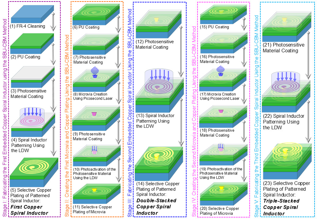
Stage II: Creating the First Microvia and Copper Plating Using the SBU-CBM Method
An additional layer of polyurethane was first spin-coated onto the SI1/HP19-1/PU1/FR-4 substrate prepared in Stage I, resulting in the substrate labeled PU2/SI1/HP19-1/PU1/FR-4. This substrate was then exposed to UV light for three minutes to cure the polyurethane. Next, photosensitive material was spin-coated onto PU2/SI1/HP19-1/PU1/FR-4, producing the substrate labeled HP19-2/PU2/SI1/HP19-1/PU1/FR-4. Immediately following the photosensitive material coating, a microvia was created using PL2210 laser machine, resulting in the substrate labeled Via1/HP19-2/PU2/SI1/HP19-1/PU1/FR-4. To enable selective copper plating of the first microvia, another layer of photosensitive material was spin-coated onto the Via1/HP19-2/PU2/SI1/HP19-1/PU1/FR-4 substrate. Selective photoactivation was then carried out using the LW405B machine with a CAD mask designed in CLEWIN software. Finally, electroless copper plating solutions were prepared according to the manufacturer’s instructions, and the substrate was immersed in the plating baths to selectively deposit copper within the first microvia.
Stage III: Fabricating the Second Embedded Copper Spiral Inductor Using the SBU-CBM Method
The procedures described in Stage I were repeated to build the second embedded copper spiral inductor. First, a new layer of photosensitive material (HP19) was spin-coated onto the Via1/HP19-2/PU2/SI1/HP19-1/PU1/FR-4 substrate from Stage II, resulting in the substrate labeled HP19-3/Via1/HP19-2/PU2/SI1/HP19-1/PU1/FR-4. The LW405B machine was then used to pattern the second spiral inductor (SI2) on HP19-3/Via1/HP19-2/PU2/SI1/HP19-1/PU1/FR-4, yielding the substrate labeled SI2/HP19-3/Via1/HP19-2/PU2/SI1/HP19-1/PU1/FR-4. After patterning, the substrate was rinsed to remove any unbonded photosensitive material. Electroless copper plating was applied to the substrate, followed by rinsing with DI water.
Stage IV: Creating the Second Microvia and Copper Plating Using the SBU-CBM Method
In Stage IV, the procedures described in Stage II were repeated to form a second microvia that provides vertical connectivity between the second and third spiral inductors. First an additional layer of polyurethane was spin-coated onto the SI2/HP19-3/Via1/HP19-2/PU2/SI1/HP19-1/PU1/FR-4 substrate prepared in Stage III, resulting in the substrate labeled PU3/SI2/HP19-3/Via1/HP19-2/PU2/SI1/HP19-1/PU1/FR-4. This substrate was then exposed to UV light for three minutes to cure the polyurethane. Next, photosensitive material was spin-coated onto PU3/SI2/HP19-3/Via1/HP19-2/PU2/SI1/HP19-1/PU1/FR-4, producing the substrate labeled HP19-4/PU3/SI2/HP19-3/Via1/HP19-2/PU2/SI1/HP19-1/PU1/FR-4. Immediately following the photosensitive material coating, a microvia was created using PL2210 laser machine, resulting in the substrate labeled Via2/HP19-4/PU3/SI2/HP19-3/Via1/HP19-2/PU2/SI1/HP19-1/PU1/FR-4. To enable selective copper plating of the second microvia, another layer of photosensitive material was spin-coated onto the Via2/HP19-4/PU3/SI2/HP19-3/Via1/HP19-2/PU2/SI1/HP19-1/PU1/FR-4 substrate. Selective photoactivation was then carried out using the LW405B machine with a CAD mask designed in CLEWIN software. Finally, electroless copper plating solutions were prepared according to the manufacturer’s instructions, and the substrate was immersed in the plating baths to selectively deposit copper within the second microvia.
Stage V: Fabricating the Third Embedded Copper Spiral Inductor Using the SBU-CBM Method
Finally, the procedures outlined in Stages I and III were repeated to create the third copper spiral inductor, thereby completing the triple-stacked structure. First, a new layer of photosensitive material (HP19) was spin-coated onto the Via2/HP19-4/PU3/SI2/HP19-3/Via1/HP19-2/PU2/SI1/HP19-1/PU1/FR-4 substrate from Stage IV, resulting in the substrate labeled HP19-5/Via2/HP19-4/PU3/SI2/HP19-3/Via1/HP19-2/PU2/SI1/HP19-1/PU1/FR-4. The LW405B machine was then used to pattern the third spiral inductor (SI2) on HP19-5/Via2/HP19-4/PU3/SI2/HP19-3/Via1/HP19-2/PU2/SI1/HP19-1/PU1/FR-4, yielding the substrate labeled SI3/ HP19-5/Via2/HP19-4/PU3/SI2/HP19-3/Via1/HP19-2/PU2/SI1/HP19-1/PU1/FR-4. After patterning, the substrate was rinsed to remove any unbonded photosensitive material. Electroless copper plating was applied to the substrate, followed by rinsing with DI water.
III. Results and Discussion
To verify that each fabrication step was precisely carried out, microscopy imaging was performed following key stages of the process. The results are presented in Fig. 3. Specifically, Fig. 3(a) shows an optical microscope image taken during Stage I, immediately after patterning using LDW and prior to metallization. This image presents the first embedded spiral inductor patterned using the LDW technique. It highlights the capability of LDW to directly define high-resolution micro-inductors within a polymeric substrate without requiring etching or masks. Fig. 3(b) displays the optical microscope image obtained at the end of Stage I, following metallization. The copper spiral inductor marked with ‘1’ in the image confirms the successful formation of the first embedded copper spiral inductor (SI1). The copper was selectively deposited along the patterned area, demonstrating precise alignment with the LDW-defined structure. Fig. 3(c) presents the top-view optical microscope image captured after Stage III, illustrating the second embedded copper spiral inductor. In this image, label “1” marks the first (bottom-layer) copper spiral inductor, while label “2” identifies the second (top-layer) copper spiral inductor. The clear distinction and alignment between the layers affirm the successful layer-by-layer build-up of the structure. Fig. 3(d) shows the optical microscope image acquired after Stage V, revealing the completed triple-stacked copper spiral inductor. Here, label “1” corresponds to the first copper spiral inductor (bottom-layer), “2” to the second copper spiral inductor (middle-layer), and “3” to the third copper spiral inductor (top-layer). The precise alignment of each copper spiral inductor indicates the robustness of the developed fabrication sequence and alignment accuracy across multiple layers. Across all stages (Fig. 3a–d), the fabricated copper strips exhibit a uniform width of approximately 10 μm, which consistent with the CAD design specifications. The SBU-CBM method shows strong potential for fabricating planar patterns with diverse lateral dimensions and geometries; feature sizes down to approximately 1 µm have been demonstrated in laboratory-scale studies, while the present work focuses on the fabrication process for the reported structure. One of the major challenges in additive manufacturing of embedded structures is achieving high selectivity during copper deposition to avoid unwanted bridging or leakage between conductive lines. The presented images clearly demonstrate that copper was deposited only in the intended spiral regions without any visible leakage or spreading between strip lines. This level of precision is a key advantage of the SBU-CBM method over conventional additive approaches. In the SBU–CBM workflow, LDW and electroless plating are coupled through a laser-defined surface-activation step that creates a chemically selective “plating template” on an otherwise nonconductive build-up polymer. After coating the substrate with a photosensitive layer, LDW locally irradiates only the CAD-defined spiral tracks. The irradiation triggers photochemical activation that induces localized polymerization and surface reactions, yielding an interfacial layer that is (at least in part) covalently anchored to the underlying polymer and enriched with metal-ion-binding functional sites. Subsequent rinsing removes non-bonded/unreacted material from non-irradiated regions, leaving a clean contrast between activated and non-activated areas. During the following activation step, catalytic species are selectively immobilized on the laser-activated regions via these binding sites and are then converted into catalytically active metallic nuclei through a controlled reduction step. When the sample is immersed in the electroless copper bath, copper deposition initiates only on these catalytic nuclei and proceeds autocatalytically, thereby producing copper solely along the LDW-written spiral geometry while suppressing deposition on non-activated background areas. This LDW-defined, catalyst-enabled selectivity is the key reason copper is deposited with high fidelity to the designed lines and without observable bridging/leakage between adjacent features. Although PU is used as the dielectric build-up layer in this study, the SBU-CBM method is compatible with a wide variety of polymeric dielectric materials commonly used in electronic packaging and is not intrinsically limited to a single dielectric formulation.
_optical_microscope_image_.tif)
To further verify the integrity and connectivity of the multilayer structure, XCT was performed using the Zeiss Xradia 620 Versa system at Luleå University of Technology. As shown in Fig. 3(e), the XCT image confirms the vertical stacking and interconnection of all three copper spiral inductors. The internal copper microvia that connects the layers is clearly visible, demonstrating the successful formation of a continuous electrical pathway through the multilayer structure. In the demonstrated multilayer structure (Fig. 3(e)), the thicknesses of the dielectric and conductive layers define the physical configuration of the stacked spiral inductors. In the present process configuration, the PU build-up layer separating adjacent spiral coils has a typical thickness in the range of ~20 µm, providing electrical insulation and mechanical support between layers. A thin residual photosensitive interfacial layer remains after laser patterning and rinsing, with a thickness on the order of a few nanometers (~5 nm), forming the immediate interface between the dielectric and the plated copper. The electrolessly deposited copper layers have a typical thickness of ~10 µm in the structures reported in this work. XCT as a non-destructive imaging technique not only validates the fabrication accuracy and structural integrity of the final inductor assembly but also provides critical insights into the spatial arrangement and encapsulation of the internal features. The successful combination of LDW patterning, selective metallization, and precise vertical interconnection underscores the effectiveness and scalability of the SBU-CBM process for fabricating high-density, multilayer embedded electronic components.
The total conductor length was extracted from the CAD layout as the centerline current path length of a single planar spiral inductor, yielding This value represents the effective electrical length over which the magnetic field is generated within one layer and includes the complete in-plane spiral trace and lateral interconnect segments. In the three-layer stacked configuration, the individual planar spirals are electrically connected in series and vertically linked by two short microvias. Assuming a microvia height of the total conductor length of the series-connected inductor stack can be approximated as
ltot≈3lspiral,1+2hvia=13.444 mm.
This formulation reflects the fact that, in a series-connected multilayer spiral, the dominant contribution to the electrical path length arises from the planar current loops, while the vertical interconnects contribute only a minor geometrical correction.
The inductance of the structure was estimated analytically using the well-established closed-form model for planar spiral inductors introduced by Mohan et al. (Mohan et al. 1999), which relates the inductance to the spiral geometry through the number of turns, the average diameter, and the fill factor:
L=μ0N2davg2[ln(2.46ρ)+0.20ρ2]In the analytical expression for the inductance, denotes the inductance of a planar spiral inductor, is the permeability of free space, and is the number of turns in the spiral. The parameters and represent the effective outer and inner diameters of the spiral, respectively, both defined along the centerline of the current path in the outermost and innermost turns. From these, the average diameter is defined as which characterizes the overall size of the current loops contributing to magnetic energy storage. The dimensionless fill factor quantifies how tightly the spiral is wound and captures the relative distribution of the current loops between the inner and outer radii. Together, these geometrical parameters determine the magnetic field distribution and stored magnetic energy, and thus govern the inductance of the planar spiral according to the closed-form model of Mohan et al. (Mohan et al. 1999)
For the spiral inductor structure reported in this work, consisting of four-turn planar spirals with an effective outer diameter of and an effective inner diameter of (approximated as circular for analytical evaluation), the calculated inductance is per planar layer. When three such spirals are vertically integrated and electrically connected in series, the total inductance increases to In this first-order analysis, the inductance contribution associated with the short vertical microvias is neglected, as the magnetic energy stored in the vertical current segments is negligible compared to that of the extended planar spiral loops. Consequently, the overall inductance is governed primarily by the planar spiral geometry and scales approximately linearly with the number of series-connected layers.
III. Conclusion
In summary, this work presents, for the first time, the fully additive fabrication of miniaturized, embedded triple-stacked copper spiral inductors using our novel Sequential Build-Up–Covalent Bonded Metallization (SBU–CBM) method. The demonstrated approach eliminates the need for vacuum systems, chemical etching, or thermal sintering while maintaining high resolution and precise vertical interconnectivity. The successful realization of three interconnected spiral inductors demonstrates the robustness and accuracy of the developed fabrication process. These structures, which feature 10 µm copper microvias and 10 µm-wide spiral strip lines, also confirm its scalability for high-density embedded components. Beyond proving manufacturing feasibility, this work highlights the critical importance of precise microvia alignment and selective metallization for achieving low-loss vertical connections and structural integrity across multiple layers. The room-temperature additive processing enabled by the SBU–CBM method provides compatibility with temperature-sensitive substrates and facilitates integration with flexible and heterogeneous electronics, while selective electroless copper plating offers a clean and mask-free approach for high-density electrical packaging. These findings position the SBU–CBM method as an enabling technology for next-generation miniaturized and embedded passive components. Such components are essential in modern electronics where compact, high-performance, and energy-efficient electronic components are required. They are particularly critical for systems supporting advanced computing hardware, AI processors, and quantum devices. Future research will focus on comprehensive electrical characterization of the fabricated inductors, integration with other passive and active components, scaling the method to larger and more complex system-in-package platforms, and exploring new substrate materials for extreme environments. The research results presented in this study set a new benchmark in embedded inductor fabrication. They open a promising pathway for the broader adoption of additive manufacturing in advanced system-in-package and integrated circuit platforms, reinforcing its potential as a key enabler of future.
Acknowledgment
The authors gratefully acknowledge the generous support of Cuptronic AB (Stockholm), whose provision of specialized materials was essential to the successful completion of this research. Sincere thanks are also extended to Fredrik Forsberg and Henrik Lycksam for their expert assistance with X-ray computed tomography (XCT) imaging, which was instrumental in validating the multilayer structures. The authors further wish to express their deep gratitude to Claudio Arnone and Jithin Thomas at MICROTECH-Italy for their invaluable guidance and technical support during the installation and operation of the LW405B laser writing machine. This work supported by the E2PackMan project, funded by the Chips Joint Undertaking and its members, with additional funding provided by Vinnova, the Swedish National Funding Authorities, under grant agreement no. 101194187. Additional support is acknowledged from the SOPRANO project, funded by the Interreg Aurora Foundation. The authors also acknowledge the critical computational support from the Swedish National Infrastructure for Computing (SNIC), with resources provided through project NAISS 2025/5-148, which enabled the modeling and analysis materials of this research.