


I. Introduction
Over the past six decades, Moore’s Law, which predicts that the transistor count on integrated circuits (ICs) doubles every 2 years, has epitomized the simultaneous miniaturization of components and expansion of functionality, driving ongoing reductions in device dimensions, enhanced performance, and deeper functional integration in semiconductor technology (Zhu et al. 2023). As device geometries have contracted from the micrometer (µm) to the nanometer (nm) scale, conventional transistor scaling has encountered fundamental limitations in lithographic resolution, power density management, and RC delays in interconnects (Schwierz and Liou 2020). To extend Moore’s Law beyond these limitations, heterogeneous integration has emerged as a vital strategy. By assembling multiple “chiplets” and die stacks into high-density 2.5D and 3D IC architectures, designers can leverage optimal process nodes, integrate specialized functions, and reduce overall system volume. However, sustaining signal integrity and managing heat in finely pitched interconnect networks demands new materials and bonding methods (Zhang et al. 2022; Wang et al. 2023).
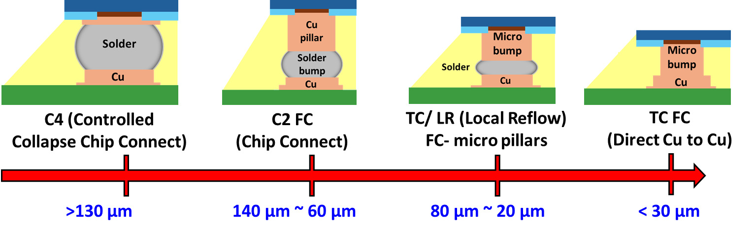
As illustrated in Figure 1, progressive miniaturization of flip-chip interconnects from >130 µm solder bumps through 60-140 µm solder-capped Cu pillars and 20-80 µm micro-bumps to <30 µm Cu-to-Cu micro-bumps enables higher I/O density (Kim et al. 2016). Cu-to-Cu direct bonding has rapidly gained prominence as a foundational technology for next-generation heterogeneous IC assemblies. Enabling ultra-fine-pitch 2.5D and 3D integrations, Cu-to-Cu bonding underpins wafer-to-wafer, die-to-wafer, and chiplet-to-chiplet interconnects with pitches well below 20 µm (Kim et al. 2016). Such direct metal-to-metal interconnects have become crucial for the development of high-bandwidth memory (HBM) stacks, compact logic-memory integrated modules, and power-intensive AI accelerators that require terabyte-per-second data throughput (Kim et al. 2022). Unlike traditional solder-based joints, Cu-to-Cu bonding eliminates the formation of intermetallic compounds (IMCs) and avoids flux-related residues, thereby simplifying the process flow and reducing contamination risks. In addition, Cu’s inherent electrical and thermal properties enable ultra-low interconnect resistance, minimizing RC delay and providing superior thermal conductivity, which is essential for efficient heat dissipation in high-density die-stacking applications (Annuar et al. 2019). Cu-to-Cu direct bonding’s high electrical and thermal performance enables high-density, high-speed, and thermally efficient topologies in modern heterogeneous IC packaging (Juang et al. 2018).
Despite its advantages, Cu-to-Cu direct bonding faces significant challenges that hinder its widespread adoption in advanced semiconductor packaging and 3D integration. A major challenge arises from the rapid formation of native Cu oxides (CuO/Cu2O), even under tightly controlled low-oxygen conditions. These insulating oxide layers hinder atomic diffusion at the bonding interface, limiting bond quality and reliability (Tseng et al. 2018). Achieving planar, oxide-free surfaces typically demands aggressive cleaning or surface activation processes, while surface activation methods like acetic acid pretreatment can remove oxides temporarily, reoxidation occurs within minutes if bonding delays exceed 3 minutes (Jang et al. 2009). Also, any residual topography, surface roughness, or planarity further complicates bonding mechanics. Electroplated Cu films typically exhibit roughness values between 3-12 nm, depending on crystal orientation, necessitating chemical-mechanical planarization (CMP) to achieve sub-10 nm smoothness for reliable thermo-compression bonding (TCB) (Liu et al. 2015). Crystallographic orientation strongly influences surface diffusion and oxidation behavior. Highly (111)-oriented nanotwinned Cu exhibits the fastest surface diffusivity while simultaneously demonstrating the lowest oxidation rate compared to (200) and randomly oriented Cu films, making it particularly advantageous for low-temperature Cu-to-Cu direct bonding (Tseng et al. 2018). Long-term reliability concerns persist due to residual interfacial defects. Void ripening occurs during thermal cycling, with grain boundary diffusion driving pore coalescence at bonded interfaces (Liu et al. 2021). Subcritical oxidation at bonding boundaries progresses over time, particularly in (100)-oriented Cu films, which oxidize 2.3× faster than (111)-oriented counterparts at 250°C (Tseng et al. 2018). These failure mechanisms necessitate comprehensive solutions addressing both initial process limitations and operational degradation pathways to enable robust Cu-to-Cu interconnects for next-generation electronic systems.
To overcome the challenges inherent to Cu-to-Cu direct bonding, industrial research has focused intensively on surface preparation and protection methods. Plasma treatments using Ar/H2 mixtures have become a common approach for removing native copper oxides by chemically reducing surface layers and sputtering contaminants away. Similarly, formic acid vapor treatments effectively reduce Cu-oxides at mild conditions, promoting clean metallic interfaces suitable for bonding (Jang et al. 2009; Yang et al. 2018). Additionally, protective metal coatings, including gold (Au), palladium (Pd) (Hong et al. 2022), and silver (Ag) (Chou et al. 2021), have been explored as diffusion barriers and oxidation-resistant capping layers, significantly enhancing surface stability and bond ability. However, despite their proven efficacy, these strategies have notable drawbacks. Plasma and formic acid cleaning typically require costly ultra-high-vacuum chambers and specialized handling equipment, thereby escalating capital investment and operational complexity. Conventional surface activation and cleaning processes can inadvertently introduce or redistribute particulate contaminants, highlighting the need for bonding strategies that minimize both chemical and particulate residues (Huang et al. 2023). Such residual contaminants and cleaning by-products pose significant challenges for ultra-fine-pitch (<10 µm) interconnects, where even trace residues or single-particle contamination can lead to localized non-bonding, open circuits, and I/O loss. These defects pose a serious reliability risk in high-density 2.5D and 3D interconnect architectures, where limited redundancy can cause localized bonding failures to directly affect overall system performance (Workman et al. 2021). The incorporation of protective metal coatings, while effective, introduces new process integration hurdles and potential intermetallic compound formation, thus complicating downstream manufacturing steps.
Additionally, maintaining precise control and consistency during cleaning treatments becomes increasingly challenging as device interconnect pitches continue to shrink. Surface activation processes designed for low-temperature bonding (typically below 200°C) are under investigation to address these issues. Still, their application in high-volume manufacturing environments remains limited due to difficulties ensuring uniform activation and long-term stability (Park and Kim 2020).
In our previous research, we addressed the persistent challenge of solder flux residue, which is difficult to remove in fine-pitch Cu-to-solder interconnects by eliminating the need for solder flux altogether (Kumar et al. 2024; Antony et al. 2025). To achieve this, we developed an ultra-thin (2-5 nm) Cu-selective oxide-suppression coating capable of significantly reducing copper oxidation at elevated bonding temperatures (250-300°C). This protective coating ensures optimal formation of intermetallic compounds (Cu6Sn5 and Cu3Sn) through enhanced Cu-Sn interdiffusion, selectively adhering to Cu while exhibiting no reactivity towards other common materials such as Al, Ni, Au, dielectric materials, or polymer substrates (Antony et al. 2025). Reliable Cu-to-Cu direct bonding is similarly impeded by copper oxidation, which disrupts atomic-scale interdiffusion and compromises bond strength. To overcome this issue, we applied the same Cu-selective ultra-thin passivation coating, deposited via industry-standard methods such as liquid-phase deposition (LPD) or chemical vapor deposition (CVD), ensuring straightforward integration into current manufacturing processes. By effectively preventing oxide formation, our passivation layer facilitates robust Cu-to-Cu bonding, without the necessity for ultra-high vacuum environments.
II. Experimental Methods and Materials
A. Chemical quantification of passivation coating and Copper oxide
Passivation coating and bonding assessments were performed on CMP-polished substrates consisting of a 2 µm-thick Cu layer electroplated over a tantalum (Ta) barrier and a silicon dioxide (SiO₂) dielectric on a Si wafer. The crystallinity of the Cu surface was characterized by grazing-incidence X-ray diffraction (GIXRD) using a Rigaku SmartLab diffractometer at a fixed incident angle of 0.5°. Surface morphology was examined using a Thermo Scientific Quattro S Environmental Scanning Electron Microscope (ESEM) operated in backscatter mode at an accelerating voltage of 10 kV. Surface roughness was quantitatively assessed using atomic force microscopy (AFM) with a Nanosurf Mobile S system.
In our prior publication, we established a robust calibration methodology to evaluate passivation coating and oxide growth on Cu surfaces quantitatively. This approach integrates Fourier-transform infrared (FT-IR) spectroscopy with Reflection Absorption IR Spectroscopy (RAIRS) and Quartz Crystal Microbalance (QCM) techniques, which respectively measure IR absorbance and coating thickness, enabling a precise correlation between spectroscopic signatures and mass-based measurements for accurate thickness quantification (Alptekin et al. 2023). Chemical bonding features of the passivation coating and Cu-oxide were identified through characteristic IR absorbance peaks, notably at 788 cm-1 for the passivation coating and 650 cm-1 for Cu-oxide. Spectral measurements were performed using a Thermo-Nicolet iS50 FTIR instrument equipped with a VeeMax II reflection accessory. To correlate absorbance and physical thickness, thickness changes data were obtained via QCM analysis using CHI 440A Potentiostat and 8 MHz quartz crystals sputtered with 99.99% Cu, followed by passivation coating and oxide growth.
Oxide suppression rate of the passivation coating was assessed by comparing uncoated (control) and passivated Cu substrates (3 samples per set) when thermally annealed on a hot plate at 300oC for 60 minutes in ambient air, simulating conditions of the TCB process to evaluate its oxidation behavior. To track oxide formation dynamics and evaluate how well the passivation layer suppressed oxidation, FT-IR measurements were taken at 5-minute intervals across the annealing duration. These findings provide a useful analysis of the thermal stability and oxidation resistance of the coated surfaces under TCB-relevant thermal stress.
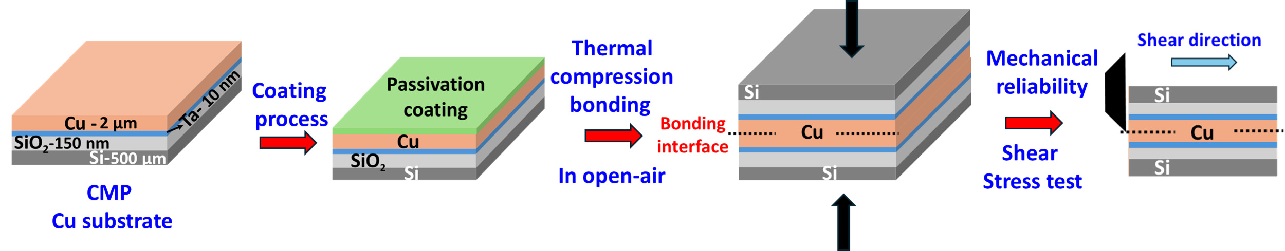
B. TCB set-up and bonding profile and shear test setup Description
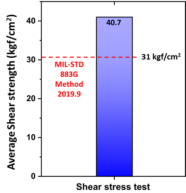
Figure 2 illustrates the process flow for evaluating passivated Cu-to-Cu bonding. The purpose-designed coating process outlined in our patent application (Kumar et al. 2024; Antony et al. 2025), was applied to Cu substrates with a bonding area of 0.5 × 0.5 cm². The coating was deposited by using either LPD or CVD, with thickness tailored by optimizing key parameters such as solution concentration, bath temperature, and coating duration. Following surface preparation, thermal compression bonding (TCB) was conducted using a lab-built thermal hydraulic press, with bonding temperatures ranging from 250 to 300°C, by applying pressures between 10 and 40 MPa, and with a bonding duration of 1 hour. A post-bond annealing step was performed at 220°C for 1 hour under ambient condition to stabilize the interface further. The bonded structures were subsequently subjected to shear stress testing to evaluate the mechanical integrity of the bonding interface. A minimum shear strength of ~31 kgf/cm² was established as the required threshold for bonded samples, calculated following the MIL-STD-883G Method 2019.7 standard (MIL-STD-883G Method 2019.8- Die Shear Strength 2019).
_scheme.png)
C. Post-bonding analysis description
Mechanical cross-sectional polishing was conducted on Cu-to-Cu bonded samples to assess interfacial bonding quality. High-resolution interface analysis was performed using a Talos F200X G2 Scanning Transmission Electron Microscope (STEM) (Thermo Fisher Scientific), operated at an accelerating voltage of 200 kV, to investigate atomic diffusion characteristics and determine any potential influence of the passivation coating on bond formation. Samples were precisely prepared using focused ion beam (FIB) milling, following the established procedure described in (Pham 2016). Elemental composition and distribution across the bonded interface were further characterized by energy-dispersive X-ray spectroscopy (EDX) mapping.
III. Results and Discussion
A. Surface Crystallinity and Morphology Analysis on Cu substrate
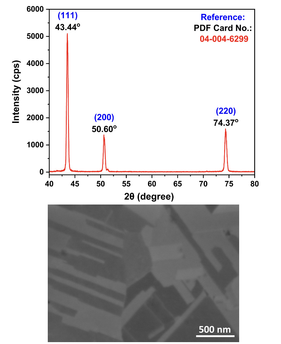
Substrates composed of CMP-polished 2 µm-thick Cu deposited over a Ta barrier and SiO2 dielectric on a silicon wafer were characterized to assess their structural and morphological properties (3 samples). As shown in Figure 3 (a), the XRD pattern exhibits sharp and well-resolved diffraction peaks at 2θ values of 43.44°, 50.60°, and 74.37°, corresponding to the (111), (200), and (220) lattice planes of face-centered cubic (FCC) Cu, indicating a high degree of crystallinity. Multiple reflections in the pattern indicate that the Cu film is composed of numerous crystals, each aligned in different directions, confirming its polycrystalline structure. The absence of secondary phases or impurity peaks further validates the phase purity of the Cu layer in agreement with the standard reference (PDF Card No.: 04-004-6299). Complementing this, the SEM image in Figure 3(b) reveals a dense and uniform surface morphology with well-defined grain boundaries and elongated grains, further supporting the polycrystalline nature of the Cu film.
_grazing_angle_xrd_pattern_and_b)_sem_backscatter_image_of_cmp_cu_substrate.png)
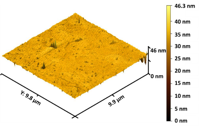
Figure 4 shows the AFM analysis (3 samples) of the CMP-polished Cu surface, captured over a 10 µm × 10 µm scan area to assess its nanoscale topography. The 3D AFM Cu surface profile demonstrates uniform roughness, with minor surface irregularities, reflecting effective planarization. The Arithmetic mean roughness over areas (Sa) was measured at 1.2 ± 0.4 nm, while the root mean square roughness over area (Sq) was 1.7 ± 0.2 nm, confirming the surface’s suitability for high-precision bonding applications.
B. Passivation coating thickness quantification
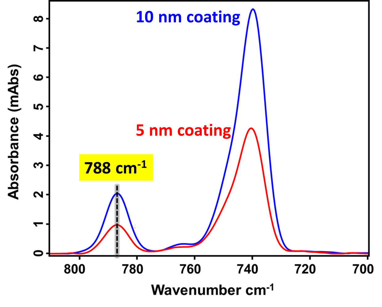
Thickness quantification for precise control of the ultra-thin passivation coating was performed using the established RAIRS-QCM metrology approach, as detailed in our previous study (Antony et al. 2025; Alptekin et al. 2023). Figure 5 presents the RAIRS spectra for Cu substrates coated with 5 nm and 10 nm passivation coatings. The absorbance at 788 cm-1 increases proportionally with coating thickness, validating the reliability of the calibration method. The distinct peak intensity variation confirms the ability of RAIRS to non-destructively resolve sub-10 nm thickness differences with high sensitivity, making it a valuable tool for monitoring ultrathin film deposition in advanced packaging processes.
C. Copper-oxide suppression quantification
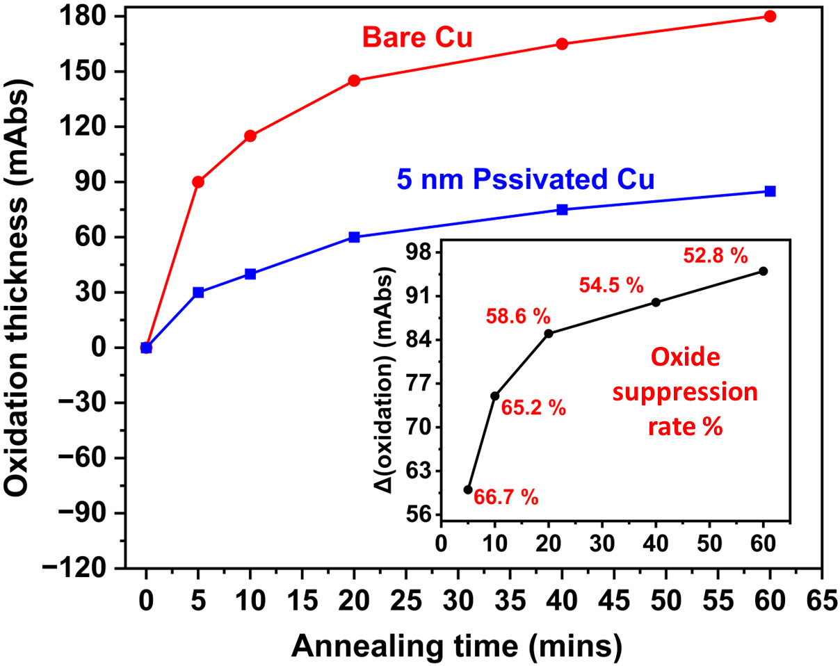
The comparative analysis of oxide growth on bare Cu and 5 nm passivated Cu substrates subjected to thermal annealing at 300°C for 60 minutes in ambient air, simulating conditions relevant to TCB. Oxide thickness was monitored using RAIRS by measuring the IR absorbance in the 650-600 cm⁻¹ range, which corresponds to the vibrational mode of Cu-oxide. The bare Cu sample exhibits a rapid increase in oxide thickness over time, reaching ~180 mAbs after 60 minutes of annealing. In contrast, the 5 nm passivated Cu sample shows significantly slower oxide growth, with a final thickness of ~86 mAbs. This represents ~53% of the oxide suppression rate, demonstrating the effectiveness of the ultra-thin passivation coating in mitigating Cu oxidation under elevated temperatures associated with bonding processes (Figure 6).

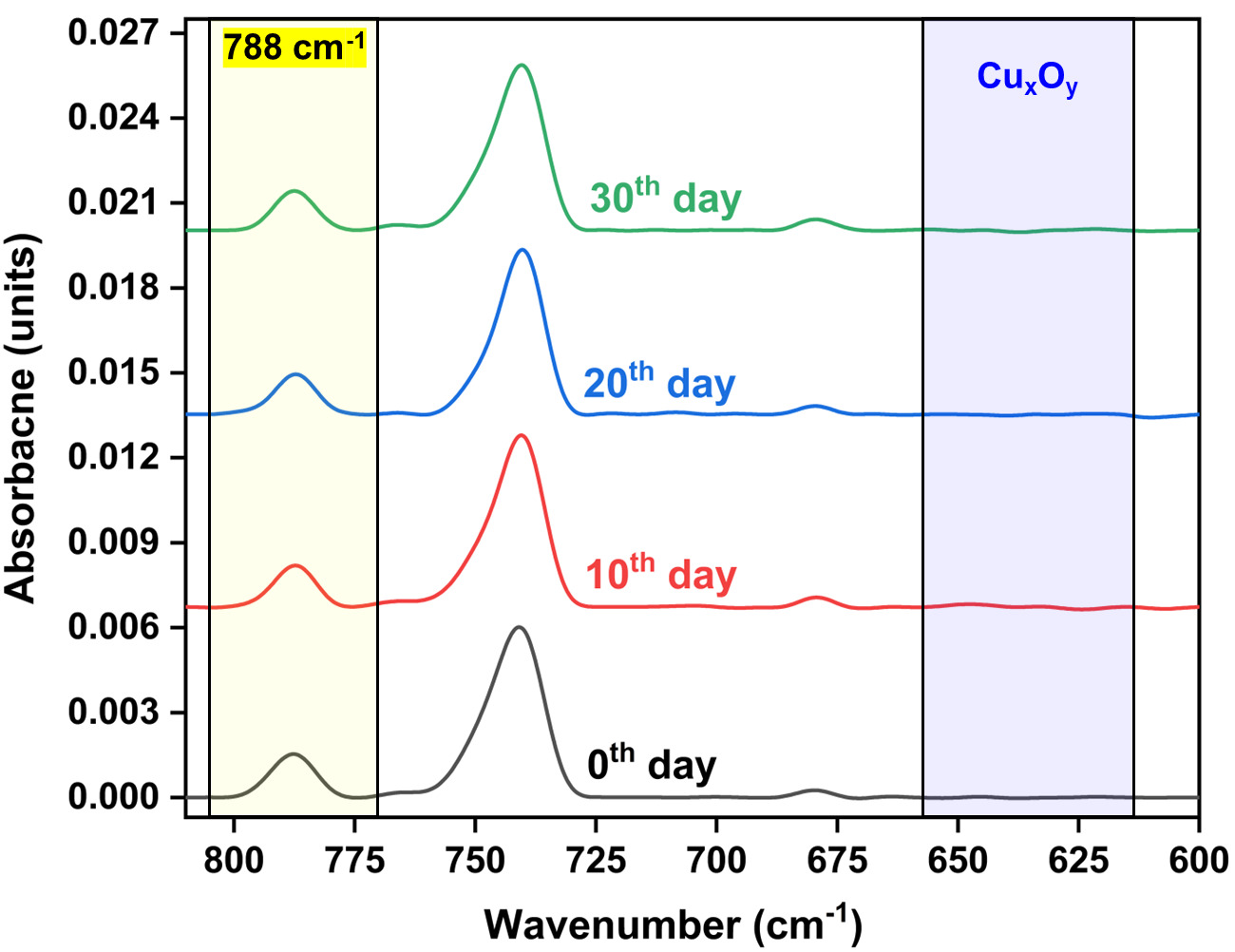
Figure 7 illustrates a time-resolved RAIRS analysis performed over a 30-day period to evaluate the long-term stability of the passivation coating on Cu substrates under ambient storage conditions. Spectra were collected at regular intervals of every 10 days and plotted to monitor changes in the characteristic absorbance features of the coating and any potential oxidation. The characteristic absorbance peak at 788 cm⁻¹, associated with the passivation layer, remains consistent in both position and intensity across all periods, indicating no significant change in coating thickness or chemical degradation. Additionally, no new peaks appear in the 650-600 cm⁻¹ region, corresponding to Cu-oxide, confirming the chemical stability and protective efficacy of the passivation coating, with no substantial degradation or oxide breakthrough even after 30 days of air exposure.
D. Post-bonding analysis and STEM/ EDX results
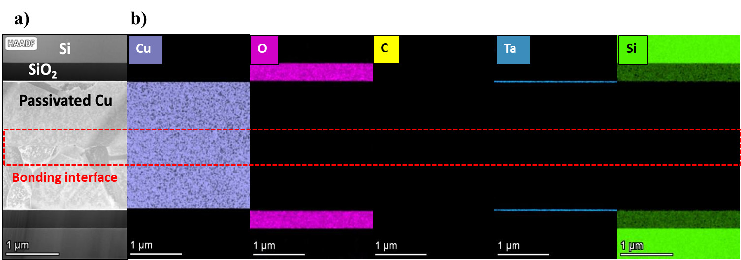
Bonding assessments using passivated Cu substrates were conducted under ambient conditions, employing optimized thermal compression bonding (TCB) for 1 hour, followed by post-annealing at 220°C for an additional hour. After bonding, the samples were cold-mounted and cross-sectioned for detailed interfacial analysis. Figure 8 presents high-angle annular dark-field (HAADF) STEM imaging along with EDX elemental mapping of the Cu-to-Cu bonded structure. The cross-sectional STEM image clearly identifies the bonding interface (highlighted in red) between the top and bottom passivated Cu substrates. Elemental mapping was performed for Cu, O, C, Ta, and Si to evaluate the interfacial composition. Notably, the oxygen (O) map exhibits no detectable signal at the bonding interface, indicating the effective suppression of oxide formation, a critical factor for reliable Cu-to-Cu bonding. Furthermore, the absence of carbon (C) signals at the interface confirms that no detectable passivation residue or contamination remains post-bonding.
_cross-sectional_stem_image_and_b)_edx_mapping_at_the_passivated_cu_to_cu_bonding_interfac.png)
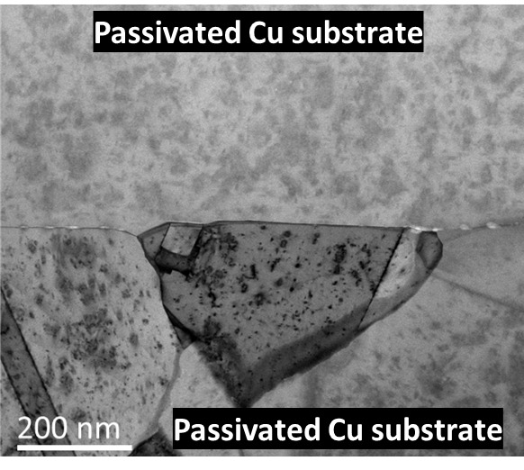
Figure 9 presents a low-angle annular dark-field (LAADF) STEM image of the Cu-to-Cu interface between passivated substrates, revealing that good contact across the Cu-Cu interface was present during TCB. This indicates effective Cu-to-Cu interdiffusion and grain growth, which are characteristic of a strong metallurgical bond. Notably, no residual passivation layer is observed, confirming unobstructed atomic transport and a clean, chemically bonded interface.
E. Shear Stress test
Following the bonding process, shear-stress testing was performed on passivated Cu substrates to assess the mechanical strength of the bonded interface. As depicted in Figure 10, the Cu-to-Cu bonded samples achieved an average (3 sample set) shear strength of 40.7 kgf/cm², surpassing the minimum threshold calculated using MIL-STD 883G Method 2019.9 for a 0.5 × 0.5 cm² bonding area. Notably, post-fracture analysis revealed that failure propagated through the silicon substrate rather than the Cu-to-Cu interface, further confirming the superior interfacial strength achieved during bonding. The absence of failure at the metallurgical junction underscores the effectiveness of the passivation strategy and its compatibility with ambient bonding conditions. These findings collectively validate the mechanical reliability and interfacial integrity of the Cu-to-Cu bonds for advanced packaging applications.
IV. Conclusion
This study presents a comprehensive approach to advancing the reliability of Cu-to-Cu direct bonding by introducing a Cu-selective, ultra-thin oxide-suppressing coating. Applied via scalable CVD or LPD, the 2 to 5 nm passivation layer significantly reduces copper oxidation during high-temperature thermal compression bonding (TCB), achieving an oxidation suppression efficiency of approximately 53% as validated by RAIRS-QCM analysis. The coating also maintains chemical integrity during ambient storage, demonstrating long-term stability without an increase in Cu oxide. Mechanical and interfacial evaluations confirmed robust bonding performance, with average shear strength (40.7 kgf/cm²) exceeding MIL-STD-883G benchmarks and STEM/EDX analyses verifying clean, oxide-free interfaces with an excellent Cu-to-Cu bonded interface. In-depth interfacial research will be pursued to elucidate the atomic-scale bonding mechanisms further and optimize coating-bond interactions. This passivation approach provides a cost-effective, high-throughput solution for fine-pitch interconnects, supporting advanced heterogeneous integration in high-performance computing and next-generation semiconductor packaging.
Acknowledgment
We would like to express our sincere gratitude to NXP Semiconductors for supplying the Cu wafers utilized in this research. Special thanks are extended to MA-tek, Taiwan, for their valuable assistance with STEM and EDX analyses. Additionally, we appreciate Dr. Usha Philipose and her team at the UNT Physics Department for their instrumental support in AFM imaging.