
I. Introduction
Radio frequency (RF) Microelectromechanical Systems (MEMS) switches have been under development for over two decades, see for example the reviews in (Tian et al. 2018; Kumar and Kumar 2021). They possess many advantages over conventional larger electromechanical relays, such as lower power consumption, smaller size and weight, higher isolation, lower loss, and faster response time, among others. Most of the current RF MEMS switch applications are at room temperature, such as telecommunications, however, there is also a growing interest in developing them for cryogenic applications such as for superconducting circuits (Tian et al. 2018; Kumar and Kumar 2021; Noel et al. 2008; Gong et al. 2009; Attar and Masnour 2015; Brown et al. 2008), space exploration (Benoit and Barker 2020) and quantum computing (Bradley et al. 2024; Sorenson et al. 2024; 2026; Lee et al. 2026; Spietz et al. 2026). Commercial off-the-shelf MEMS switches offer significant benefits over custom MEMS, such as reduced costs which increases the scalability of their use in commercial applications. Recent work by Lee et al. (Lee et al. 2026) and Spietz et al. (Spietz et al. 2026) evaluated the RF performance of commercially available and hermetically packaged RF MEMS switches at temperatures below 10 K. Commercial switches are packaged inside hermetically sealed housings which provide environmental protection for the MEMS, but which also prevent use of scanning electron microscopy for inspection and identification of potential device wear and damage. Thus, in addition to RF characterizations, there is a need to develop metrology to evaluate the reliability and repeatability of hermetically packaged MEMS switches at cryogenic temperatures.
Previous work at NIST (Bradley et al. 2024; Sorenson et al. 2024; 2026) describes a test apparatus and DC electrical protocols for reliability testing of electrostatically actuated commercial MEMS switches as a function of temperature down to ~17 K. The present work extends the test methods to evaluate the lifetime (number of switching cycles to failure) at different cryogenic temperatures and measures changes in the DC characteristics over the lifetime at those temperatures. The test techniques were performed on two sets of hermetically packaged, commercially available, RF MEMS switches from the same manufacturer as in Refs (Lee et al. 2026; Spietz et al. 2026). Whereas Refs (Lee et al. 2026; Spietz et al. 2026) evaluated the RF performance of the switches, the present work focuses on the switches’ mechanical and DC reliability. The goal of this work is reliability testing of cryogenic MEMS switches, with this commercial MEMS switch being a test vehicle for metrology development. The motivation is to provide MEMS switch users and manufacturers with reliability test methods to aid in the deployment and development of MEMS switches for cryogenic environments.
II. Experimental Methods
A. Experimental set-up
All tests were performed in a custom Gifford-McMahon (GM) cooled cryogenic chamber. The cryostat had two cooling stages instrumented with heaters and thermocouples and was set at a vacuum pressure of 10-4 Torr (0.013 Pa). The two cooling stages could be independently controlled to achieve the desired cooling rates and arbitrarily selected equilibrium temperatures. The minimum second stage temperature was ~17 K with the first stage minimum of ~60 K. On each stage, instrumented machined copper fixtures held the printed circuit boards (PCB) on which the MEMS chip-scale packages were mounted. The copper fixtures served to provide thermal conduction between the cooling stages and the MEMS package. The fixture lifted the entire board above the baseplate, suspending the board’s metal traces and electrical ports above the baseplate, thus electrically isolating the MEMS from the cooling stage. Surrounding the cooling stages were radiation shields. Thermocouples were attached to the cooling stages, the copper thermal adapters, the MEMS PCBs, and the top of the MEMS chip packages. Details about this test apparatus were reported in the previous NIST works (Bradley et al. 2024; Sorenson et al. 2026). The measurement uncertainties in the voltage, contact resistance, and temperature for all tests were 0.1 V, 0.001 Ohm, and 0.1 K, respectively.
B. Test protocols
The two sets of RF MEMS switches were simultaneously cooled and tested. One set of switches (on board “A”) was cooled to 17 K and the other set (board “B”) to 60 K. Other temperatures could also be used if desired. Each channel on the MEMS PCB was then turned on and off at a rate of 7 kHz using a drive voltage of 90 V. At repeated intervals – ranging from several hundred thousand switching cycles to several million cycles – the on/off cycles were paused and the switches’ response to the drive voltage was observed to determine if they were still functional or had “failed”. Failure was defined as when an output channel could not switch states.
While still cooled, the remaining functional switches (channels) were characterized with the suite of tests described in (Bradley et al. 2024; Sorenson et al. 2026), including measurements of hysteresis when cold-switched, hysteresis when hot-switched, switching response time and measurement of the drift in contact resistance when held closed for up to an hour. In the cold-switching hysteresis test the drive voltage was swept from 50 V to 90 V and back to 50 V at a rate of 1 V/s while the contact resistance was measured in a four-probe configuration. In the hot-switching hysteresis test a DC carrier signal was applied to the channel’s input and the output was measured as the drive voltage was similarly swept. To measure the switching response time, a 0.5 VDC carrier signal was applied to the channel input, and the time for the output signal to reach steady state when a 90 VDC actuation step voltage was turned on and off was measured. In the “resistance creep” (drift in contact resistance) test, the switch was kept closed for up to an hour and the contact resistance measured once per minute. These DC characterization test methods are described in more detail in the previous NIST works (Bradley et al. 2024; Sorenson et al. 2024; 2026) where these measurements were taken as a function of temperature from room temperature down to 55 K (Bradley et al. 2024) and 18 K (Sorenson et al. 2024; 2026). The present work measured these characteristics as a function of the number of on/off switching cycles at fixed temperatures. This paper presents a subset of the lifetime test results.
Failed switches were stuck in either the closed or open position which was determined through contact resistance measurement. Unlike room-temperature operation, MEMS switches which failed as stuck-closed can sometimes be fixed if the stiction failure was caused by a buildup of charges due to the lower charge dissipation rate at cryogenic temperature (Benoit and Barker 2020) or if due to the effects of the thermodynamic properties of the gases enclosed in the MEMS housing, both issues are discussed in the section on experimental results. Other causes of failure, such as due to wear of the contact surfaces or material deformations and fatigue, are not fixable. When irreversible factors largely accumulate, the switch does not recover and is permanently non-functional.
In the present work, failed switches were either allowed to warm up or were kept cooled for 24 hours. If a switch was found to be operational again after these interventions, if needed it was re-cooled to the test temperature and put through the suite of DC characterization tests before the on/off cycling was resumed until failure was observed again.
With this lifetime test protocol, the conditions under which switches fail and “recover”, and the cumulative number of cycles until failure was not recoverable, can be determined. Changes in each switch’s DC electromechanical characteristics leading up to the failures and before and after the interventions were also recorded. This test method generates a large set of systematic data for evaluating MEMS switch reliability at various steady-state cryogenic temperatures.
C. Devices under test
As a demonstration of these cryogenic MEMS reliability test methods, tests were performed on two identical commercially available single-pole-four-throw RF MEMS switches, manufactured from the same commercial process as the devices investigated by Spietz et al. at temperatures from 25 mK to 3 K (Spietz et al. 2026) and by Lee et al. at 5 K (Lee et al. 2026). However, whereas (Lee et al. 2026; Spietz et al. 2026) focus on the RF characteristics of these MEMS switches, the present work focuses on the lifetime (cycles to failure) and DC characteristics, and at higher cryogenic temperatures (17 K and 60 K).
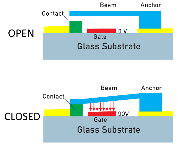
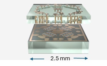
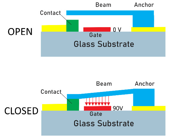
Each test vehicle was a 2.5 mm x 2.5 mm glass chip-scale package mounted on a PCB. Each glass package contained 32 electrostatically actuated MEMS cantilever beams on a glass substrate. The cantilever structural material is a highly conductive proprietary metal alloy. The glass substrate also contains conductive metal traces, contact pads and through-glass-vias for external connection. When no actuation voltage is applied, each cantilever beam in its resting state is suspended above the substrate. When 90V is applied, the electrostatic force from the voltage pulls the beam down to the substrate, forming a metal-to-metal contact between the input and output ports, as shown in Figure 1.
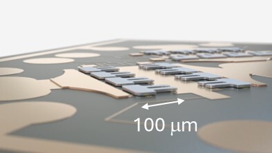
The 32 MEMS cantilevers are arranged into 4 output channels. Each channel consists of 8 individual cantilever-based unit cells measuring approximately 100 micrometers x 100 micrometers each, arranged as four in parallel and two in series, see Figures 2 and 3. A glass cover is hermetically bonded to the glass substrate thereby enclosing the MEMS in a proprietary gas mixture optimized for RF performance and long-term stability. At cryogenic temperatures, however, the gas condenses and solidifies, thus making it critical to evaluate potential variations in the device performance under cryogenic conditions (Menlo-Microsystems 2025; n.d.). For example, Lee et al (Lee et al. 2026). observed bouncing of the cantilevers when the switches opened and closed in response to a 10 kHz step voltage at 5 K and attributed the bounce to condensation of oxygen and nitrogen creating a partial vacuum inside the glass package.
_of_the_commercial_single-pole-four-t.jpeg)
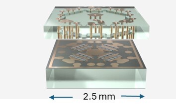
Each 2.5 mm x 2.5 mm glass package was mounted (by the manufacturer) on a 38.1 mm x 63.5 mm PCB with RF transmission lines and SMA connectors. In this work, one PCB was designated “A” and the other “B”. Each switch (output channel) on each board was given a number. Thus, for example, “B1” refers to channel 1 on board B. A separate PCB from the manufacturer, containing the MEMS control circuitry, was used to cycle the switches on/off at a rate of 7 kHz.
Note that in the manufacturer’s product literature, the “single-pole-four-throw switch” refers to the entire 2.5 mm x 2.5 mm glass package with 4 output channels as shown in Fig 3. In this work, each channel is referred to as a separate switch, i.e., each 2.5 mm x 2.5 mm glass package is considered as four individual MEMS-based switches. Note further that each channel – and thereby each “MEMS-based switch” – further consists physically of 8 cantilevers or unit cells, as in Fig 2. Since the 8 cantilevers are electrically connected, each set of 8 cells is distinguished as a single MEMS-based switch.
III. Results
A. Temperature-related trends
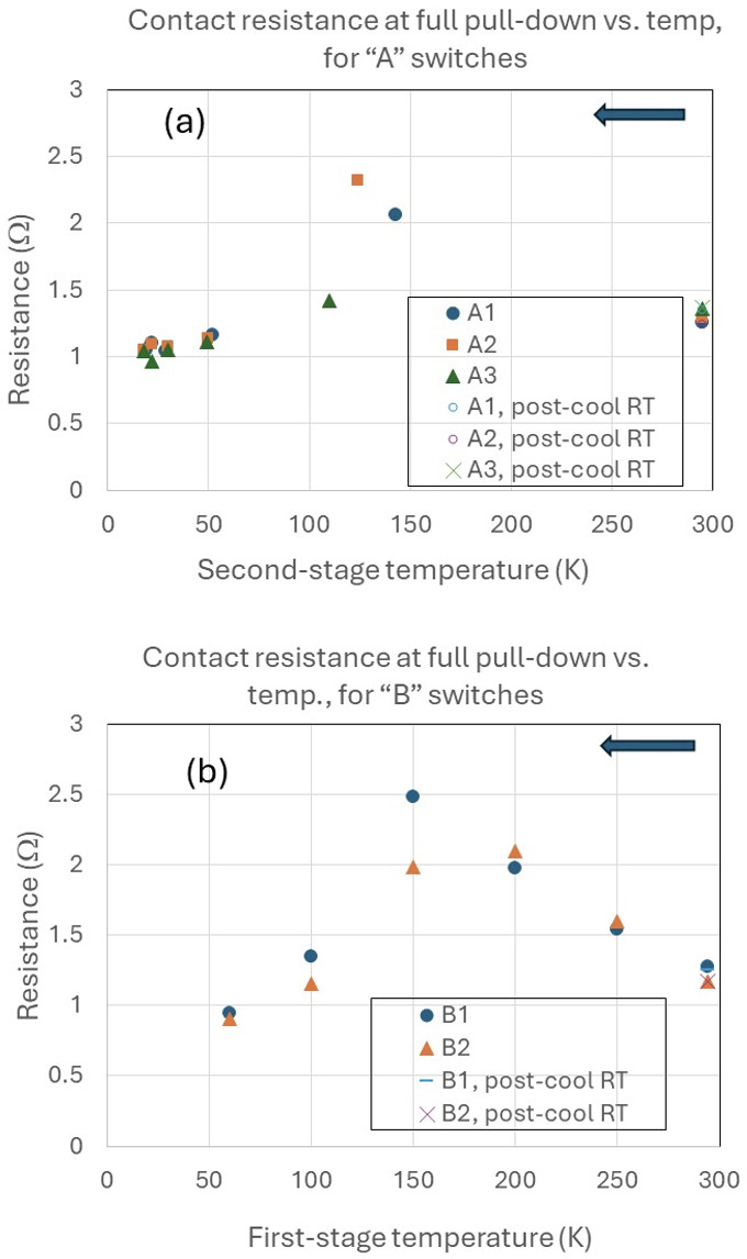
The previous NIST work (Bradley et al. 2024; Sorenson et al. 2024; 2026) found several of the DC characteristics of the MEMS switches to vary with temperature. Similarly, Figure 4 shows that the contact resistance during the cold-switching hysteresis test, for each switch (channel), increased when cooled from room temperature to ~100 K – 150 K, and then decreased when further cooled from 100 K to 17 K. This “inverted U”-shaped trend of the resistance with temperature contrasts with previous studies in the literature on cryogenic RF MEMS switches (such as [Noel et al. 2008; Gong et al. 2009; Attar and Masnour 2015; Brown et al. 2008; Benoit and Barker 2020]) which featured un-packaged MEMS switches. Those studies reported monotonically increasing contact resistance with decreasing temperature due to the cantilever material stiffening at low temperatures. On the other hand, Lee et al (Lee et al. 2026)., who did RF characterization of the MEMS switches from the same manufacturer as in this work, also measured their switches’ contact resistance and found it to be 15% lower at 5 K than at room temperature, a result that agrees with Fig 4, and they attributed this to the reduced phonon scattering at 5 K. However, as their resistance measurements were at one cryogenic temperature (5 K), the “inverted U”-shaped temperature-dependence of the resistance shown in Fig 4 was not observed in Ref (Lee et al. 2026).
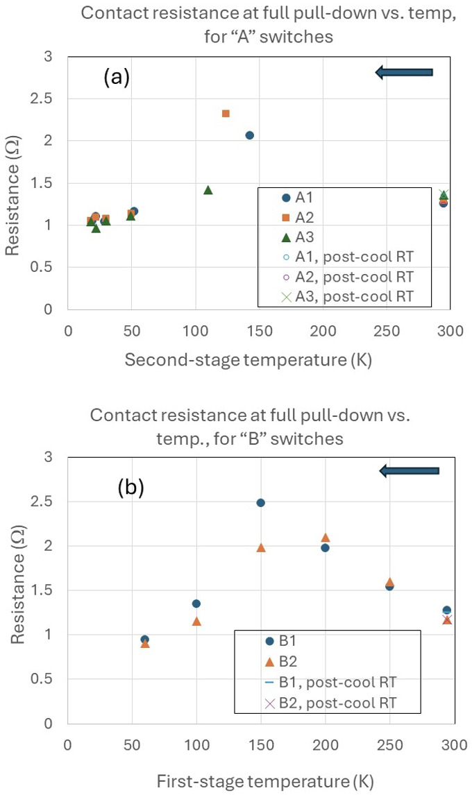
The repeatability of the present measurements suggests thermodynamic effects of the gas in the hermetically sealed glass package as a possible explanation for the inverted U-shaped plot in Fig 4. The peak of the graph (at temperature of 100 K – 150 K) which represents a change in the direction of the resistance with temperature, appears to correspond to the boiling point of oxygen, which is ~ 90 K at standard atmospheric pressure. Below 100 K, condensation of oxygen on the switch’s contact surfaces might create liquid capillary forces acting on the MEMS cantilevers to increase the cantilever beams’ surface area in contact with the substrate thus lowering the contact resistance. With further cooling below 77 K nitrogen also condenses, adding more capillary force to the beams and further reducing the contact resistance. When the test chamber warms back up, the nitrogen and oxygen in the chip package undergo the phase transition back into gas, thus eliminating the capillary forces acting on the beams and increasing the resistance. Above 150 K the contact resistance decreases with increasing temperature as the higher temperatures reduce the stiffness of the beams. Other contributing factors to the inverted U-shaped plots in Fig 4 could be temperature-dependent stresses due to coefficients of thermal expansion/contraction resulting in warping of the substrate or deformation of the beams.
Refs (Bradley et al. 2024; Sorenson et al. 2026) show temperature-related trends of other measured DC characteristics such as the drift in the contact resistance over time when the switches were kept closed for up to an hour at different temperatures (which also showed a similar inverted U-shaped plot with the peak around 150 K [Bradley et al. 2024]), as well as the hysteresis curves during hot switching and cold switching, and the switching times.
Since from Fig 4 the highest resistance and the widest scatter in the resistance measurements occurred at 100 K to 150 K, possibly due to the phase transition of oxygen in the glass package as discussed above, the lifetime (on/off cycling) tests described in the next section were performed at 17 K and 60 K where the resistances were lower and more stable.
B. Cycles to failure at 17 K and 60 K
Board A was cooled to a steady state temperature of 17 K, while board B was simultaneously cooled to 60 K. While holding each board at its steady state temperature, the switches (channels) were cycled on and off at a rate of 7 kHz using the manufacturer-recommended step voltage of 90 V. Failure is defined as when a switch (channel) failed to either turn on or off. It was found that at 17 K most failures were of the “stuck closed” type, but the switches were able to open again when the temperature increased to 41 K, or when the switches were kept at the test temperature overnight. Thus, the initial stiction failures were reversible, akin to the observations reported by Benoit et al (Benoit and Barker 2020). for their non-commercial and non-packaged RF MEMS switches actuated for 10 million cycles at 5 K. Benoit et al. identified charge accumulation in the substrate as the cause of their stiction failure at low temperature. Charge build up at 17 K from repeated cycling is likely to be the cause of the stiction failures in the present work as well, given that the stiction was non-permanent and the switches regained functionality when the temperature was increased or the switches were kept overnight at 17 K, as both situations would allow the trapped charges to dissipate and free the beams. In the present work, the failed switches recovered and were cycled again to failure. Failure followed by recovery occurred several times per switch with continued cycling. Table 1 summarizes the number of cycles to the first failure.
From Table 1, the switches cycled at 17 K failed in the closed position for the first time between 50 million to 150 million cycles but recovered and were operational again. With continued cycling, these switches failed and recovered several more times. The “B” switch that was cycled at 60 K still had not failed after 3.1 billion cycles when this test campaign concluded, but its hysteresis characteristics showed trends that preceded the “A” switches’ failures, which suggests impending failure at 60 K, as discussed in the next section.
C. Characterization tests vs. cycles at 17 K and 60 K
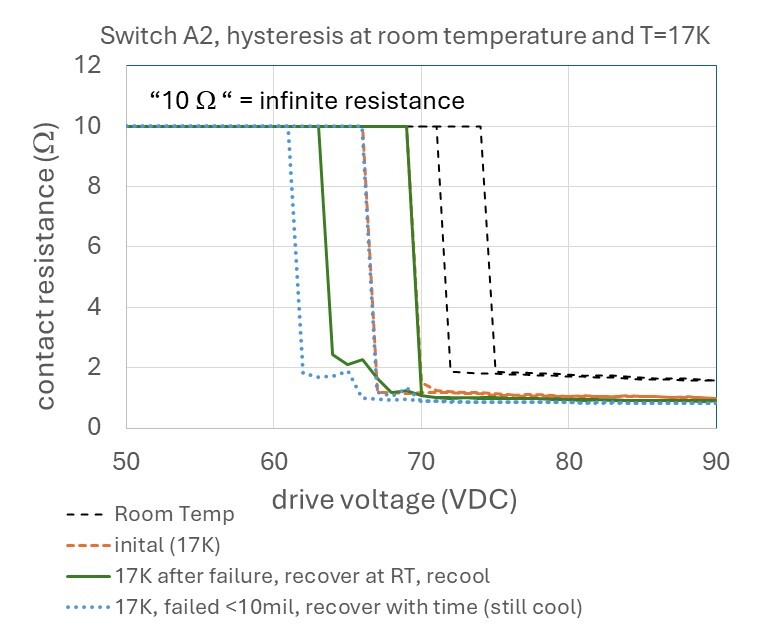
As mentioned in previous sections, one of the characterization tests is the measurement of the hysteresis in the drive voltage. In this test, we sweep the drive voltage from 50V to 90V and back while measuring the contact resistance, details are in (Bradley et al. 2024; Sorenson et al. 2026). Figure 5 shows hysteresis curves measured for one switch (A2) at room temperature, then at 17 K before the start of the on/off cycling, then at 17 K before and after initial cryogenic stiction failure from cycling, and then after a recovery and second failure after more cycles. Fig 5 shows that the switch’s hysteresis is sensitive not only to temperature but also to the number of switching cycles at fixed cryogenic temperature. Plots for the other switches are similar.
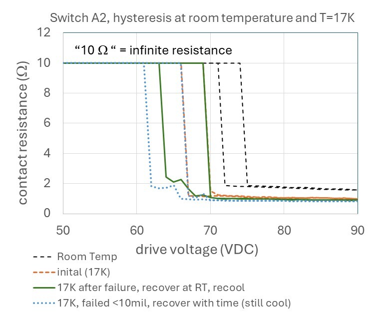
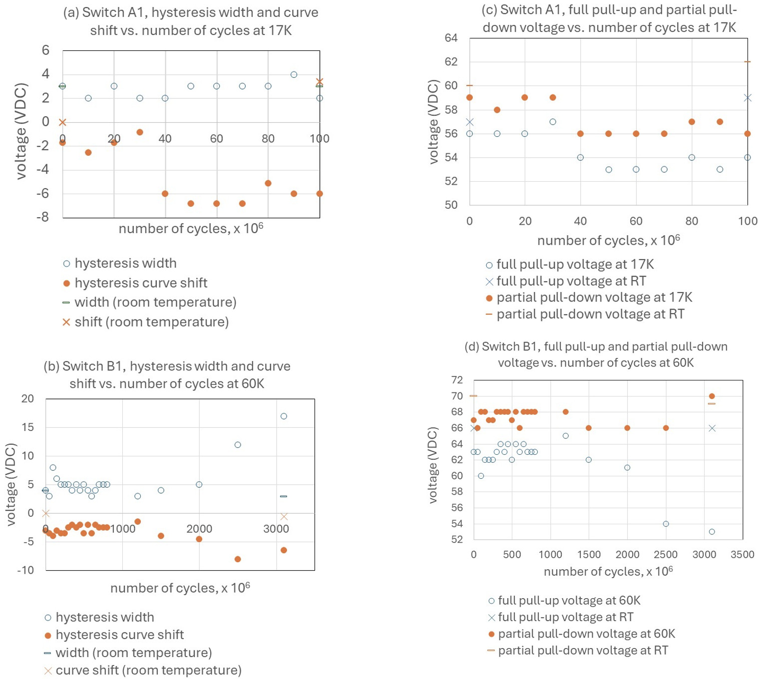
Given that the hysteresis curve is sensitive to the number of switching cycles (Fig 5), throughout the lifetime tests the cycling was periodically paused and the hysteresis remeasured at the cycling temperature. We define the voltage at which the switch closes, and the resistance becomes non-infinite, as the “partial pull-down” voltage. As the voltage is increased the resulting firmer contact results in a lower resistance. The “full pull-down” voltage is the voltage at which the resistance reaches its minimum. The measured full pull-down voltage was 90V, which corresponded to the manufacturer’s recommended voltage to close the switch. The “full pull-up voltage” is the voltage at which the closed switch fully opens and the resistance is infinite. The width of the hysteresis curve is the difference between the partial pull-down voltage and the pull-up voltage. The shift of the curve is the difference between that curve’s center voltage with respect to the center voltage measured at room temperature. More details of the hysteresis test protocol are in Refs (Bradley et al. 2024; Sorenson et al. 2026).
Figure 6(a) and (b) shows that the hysteresis width and shift are sensitive to the number of switching cycles at low temperature, and that the increasing magnitude of the width and shift could be a predictor of impending failure. Fig 6(c) and (d) show the corresponding partial pull-down and full pull-up voltages.
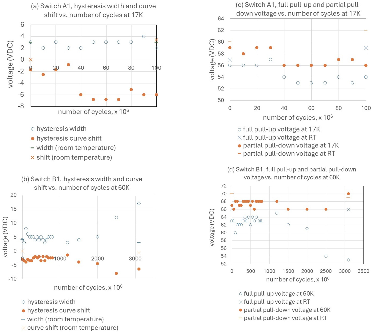
Reliability-related factors that simultaneously affect both the pull-down and pull-up voltages might not change the hysteresis width. For example, if fatigue cracks formed in the beams, one might expect both the pull-down and pull-up voltages to decrease with increasing number of cycles. If work hardening of the metal beams has occurred, the pull-down and pull-up voltages would both increase due to increased beam stiffness. From Fig 6(c), switch A1 might have undergone work hardening from 70 million to 80 million cycles. The hysteresis curves for a different switch (A2) shown in Fig 5 show that its pull-down and pull-up voltages both decreased after two stiction failures and recoveries (represented by the dotted line with the smallest dots in Fig 5), so this switch might have fatigued. It should also be noted that as mentioned in Section II.C, each “switch” or channel is actually comprised of 8 MEMS cantilevers electrically connected to each other for redundancy. Therefore, it is possible that fatigue or work hardening might occur in a few cantilevers within a switch or channel but without impacting the aggregate performance of the 8 beams. Future work will include visual inspection of the cantilevers after lifetime testing, such as by use of x-ray tomography or cross-sectioning followed by scanning electron microscopy.
Mismatches in coefficients of thermal expansion/contraction (CTE) between the MEMS cantilevers and the substrate and package might also cause temperature-dependent warping which could change the gap between the beams and the substrate and thereby shift the pull-down and pull-up voltages. Given that the switching cycles in this work were done at fixed temperature, however, changes in pull-up and pull-down voltages with increasing number of cycles are unlikely to be due to CTE mismatch.
Another cause of decreasing pull-down voltage is not mechanical in nature but rather is due to charge trapping in the substrate, which increases at low temperatures. After 100 million cycles at 17 K, switch A1’s hysteresis curve was remeasured at 17 K and then at room temperature. Fig 6(c) shows that the room-temperature pull-down voltage increased by ~ 11% compared to at 17 K, while the pull-up voltage increased by ~ 9%. Switch B1 (Fig 6(d)) shows a similar trend where both the pull-down and pull-up voltages decreased after 1.2 billion cycles at 60 K, then after 3.1 billion cycles the pull-up voltage increased substantially (by 24%) at room temperature compared to at 60 K. (B1’s pull-down voltage after 3.1 billion cycles showed a decrease from 70V at 17 K to 69V at room temperature. (It is unclear why B1’s pull-down voltage after 3.5 billion cycles is slightly lower at room temperature compared to at 60 K.)
The lower pull-down voltage at 17 K compared to at room temperature after cycling (Fig 6(c)), as well as the “recovery” of the cryogenic stiction failures when the temperature was subsequently increased, are similar to observations reported by Benoit et al (Benoit and Barker 2020). for their (non-commercial and non-packaged) MEMS switches tested at 5 K. Benoit et al. identified charge trapping as the cause of both phenomena. Lee et al (Benoit and Barker 2020). also observed a decrease in their pull-down voltages at 5 K. As with Benoit et al (Benoit and Barker 2020)., charge accumulation from repeated on/off cycles at fixed temperature is likely the cause of the decrease in pull-down and pull-up voltages between 0 and 40 million cycles at 17 K in Fig 6(c), as well as the stiction failures which were reversed with increased temperature (Table 1).
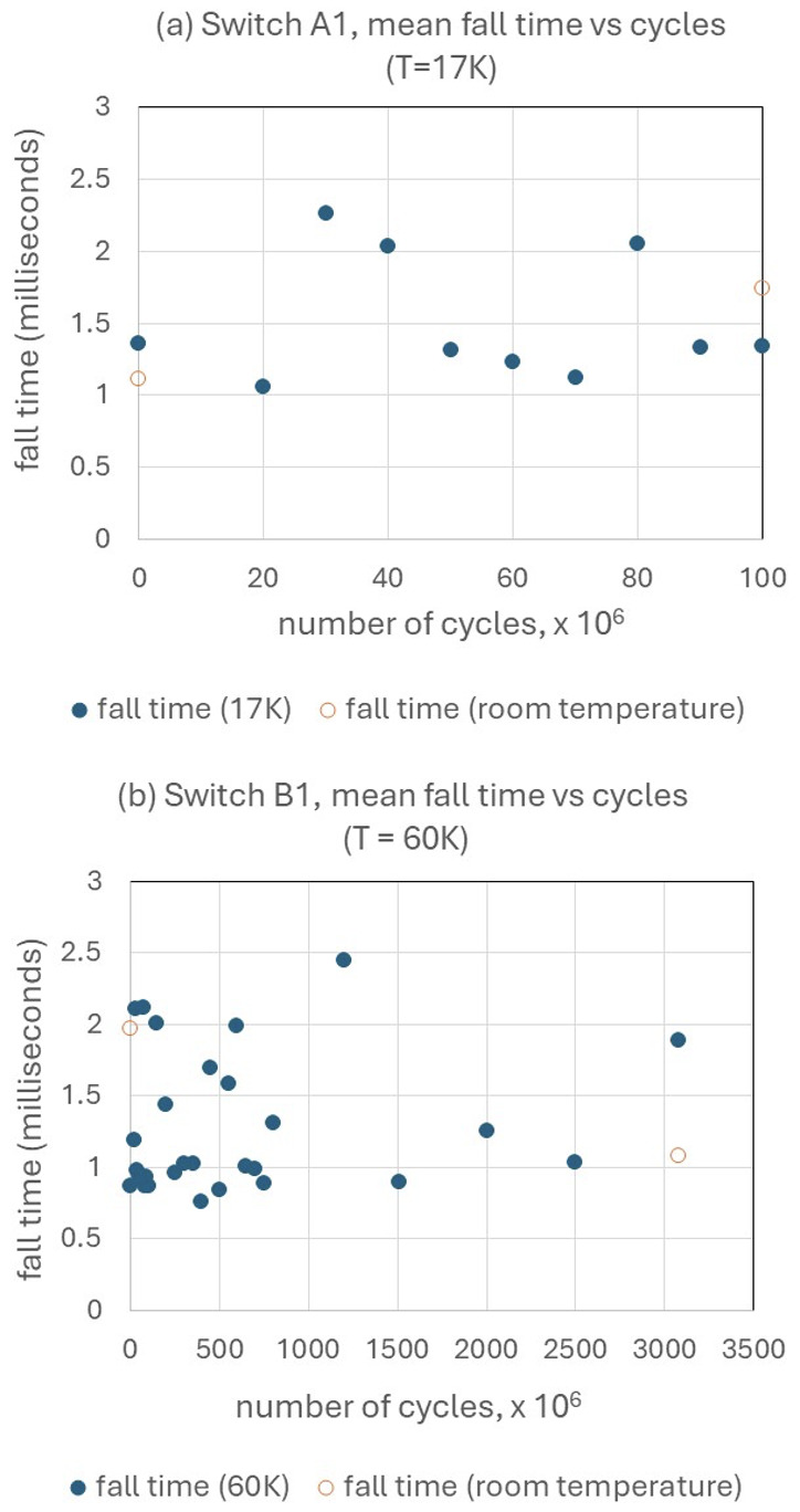
Another characterization test is the measurement of the switch’s response time to a 90V step input, details of this test protocol are in Ref (Sorenson et al. 2026). In this work, the time for a 0.5 VDC carrier signal to increase from 0 V to 0.5 V (the rise time) when the switch is turned on was measured, and the time for the signal to drop to 20% of its full value when the switch is turned off (the fall time) was also measured (whereas in Ref [Sorenson et al. 2026] the fall time was taken as the time for the carrier signal to reach 0V). The sampling rate was 100 kHz. These measurements were taken independently of the cycling intervals, i.e., the rise and fall times were not measured while the switches were cycled, but while actuated with a 0.5 Hz square wave during pauses in the cycling.
Unlike the hysteresis tests, the rise times and fall times did not show noticeable changes with the number of switching cycles. For example, Figure 7 shows the fall times for the “A” and “B” switches varied between 1 – 2.5 milliseconds throughout the lifetime tests. Similarly (but not shown in these graphs), the rise times of all switches varied between 10 – 20 microseconds throughout the lifetime testing at 17 K and 60 K. In previous work (Sorenson et al. 2026), the rise and fall times of these switches were also found to be independent of temperature from room temperature down to 18 K.
_one_switch_cycled_at_temperature_17_k__(b.png)
As mentioned before, the rise and fall times were measured in between cycling intervals. Since the cycling rate was 7 kHz, and the measured fall time for a step input was 1 - 2 milliseconds, the switches therefore were likely not fully open or closed during cycling, which could result in the switches bouncing. Lee et al (Lee et al. 2026). found that when they cycled their MEMS switches (from same manufacturer as in the present work) at a rate of 10 kHz and temperature of 5 K, their switches bounced when actuated with a square wave. They measured total initial fall times, including bouncing, of ~ 150 microseconds, and attributed the bouncing to condensation of the gases in the package creating a partial vacuum. They eliminated the bounce replacing the square wave with an engineered waveform as the drive function. Since the objective of the present work is to evaluate the switch lifetime, beam bouncing would increase the wear on the contact surfaces and result in more conservative values of lifetime. Nevertheless, future work will use a slower cycling rate to avoid the potential for bouncing.
IV. Discussion
In this section we discuss how this work compares with the literature on cryogenic RF MEMS switches in general, and with the recent works by Lee et al (Lee et al. 2026). and Spietz et al (Spietz et al. 2026). who both used commercial fully packaged MEMS switches from the same manufacturer as in the present work. We then put the present work in context with our previous work (Bradley et al. 2024; Sorenson et al. 2024; 2026).
A. Comparison to test methods in the literature
A major difference between our test methods (Refs [Bradley et al. 2024; Sorenson et al. 2024; 2026] and the current work) and the test methods used in the cryogenic RF MEMS switch literature (such as but not limited to Refs [Noel et al. 2008; Gong et al. 2009; Attar and Masnour 2015; Brown et al. 2008; Benoit and Barker 2020; Lee et al. 2026; Spietz et al. 2026]) is the temperature range. Most of the literature show tests at temperatures below 10 K, and/or at a single cryogenic temperature in that range, while Brown et al (Brown et al. 2008). did tests at 77 K, Spietz et al (Menlo-Microsystems, n.d.). did their measurements in a dilution refrigerator at four temperatures between 25 mK and 3 K, and Lee et al (Menlo-Microsystems 2025). performed RF characterizations at 5 K and their dynamic (switching time) measurements at ten temperatures between 10 K and 100 K. Our test methods, on the other hand, used ten steady state temperatures from room temperature to 17 K, thus our test methods cover a broader and higher temperature range, which complements the literature works and reveal different temperature-dependent effects not reported in the other papers, such as the “inverted U” shape of the contact resistance vs. temperature plots in Fig 4. (Aside from this work and Refs [Lee et al. 2026; Spietz et al. 2026], the cryogenic MEMS switches in the literature were not packaged. Un-packaged MEMS switches may not show the same trend as in Fig 4 even if tested over the same temperature range, since the “U” shape is attributed to condensation of gases in the MEMS chip package.)
Aside from the temperature range, the more fundamental difference between our work and that in the literature including (Lee et al. 2026) and (Spietz et al. 2026), lies in the objective, which motivates the differences in test methods. The literature works share an overarching objective of developing and demonstrating better-performing cryogenic RF MEMS switches or switch-based assemblies, whether it be through innovations in the MEMS design, materials, fabrication processes, circuit designs, control methods, architectures or system integration approaches. Their test methods therefore focus primarily on RF characterization, with DC tests typically involving limited numbers of measurements of the pull-down voltage, contact resistance, and number of cycles to failure. Some papers, such as Benoit et al (Benoit and Barker 2020)., also include scanning electron microscope images for visual inspection of the wear of the contact surfaces after failure.
By contrast, the objective in this work and our previous work (Bradley et al. 2024; Sorenson et al. 2024; 2026) is not on improving the switch technology or RF performance, but on methods to evaluate any electrostatically actuated MEMS switch’s reliability at cryogenic temperatures. The term “reliability” is used frequently in the literature and is universally taken to mean the number of on/off cycles until a switch is stuck in the closed or open position, at which point the switch is considered to have “failed”. Many papers show lifetime testing via on/off cycling to failure. In contrast, we consider reliability to include more than just failure, but also whether the failures are reversible, and how reproducible the characteristics of multiple “identical” switches are, as well as the gradual and cumulative changes in their operating characteristics that could affect the repeatability of their performance. For example, even if a MEMS switch still opens and closes, any increases or variability in the contact resistance or switching time or drive voltage could adversely impact its usefulness. Our test apparatus (Bradley et al. 2024; Sorenson et al. 2026) is therefore designed for automated tests of two MEMS boards (with four switches or channels per board) simultaneously over a broad range of independently adjustable steady state temperatures to efficiently collect data on the DC characteristics at different cryogenic temperatures and with repeated cycles.
We use DC rather than RF characterizations because MEMS switches are basically cantilevers that alternate between two mechanically stable positions, thus switch reliability is primarily impacted by mechanical reliability. Whereas RF measurements are highly sensitive to electrical parameters within the test system such as impedance matching and parasitic capacitances and inductances, DC tests are electrically less complex and are thus more directly correlated with the mechanical behavior. Furthermore, changes in the switch characteristics that are temperature-dependent and reversible (such as from charge trapping or CTE mismatch stresses), versus permanent and cumulative (such as due to fatigue or work hardening of the beam), add another set of considerations for MEMS switch users and manufacturers. Therefore, our reliability test methods focus on not just switch failure but also on measuring changes in mechanical and DC characteristics with respect to temperature, number of switching cycles, number of cooling cycles (Bradley et al. 2024; Sorenson et al. 2024; 2026), and across multiple switches.
All the above factors apply to a comparison between our test methods and that of Lee et al (Lee et al. 2026). and Spietz et al (Spietz et al. 2026). who both did recent tests of commercial fully packaged RF MEMS switches from the same manufacturer as in this work. Their tests were done at lower temperatures and focused on RF characterizations, and Lee et al. also performed logic operation tests and some DC tests, while Spietz et al. did RF calibrations. Our DC reliability test methods therefore complement the test methods used in their works.
For a comparison of the DC test methods in (Lee et al. 2026) with our work, Lee et al (Lee et al. 2026). also measured the switching time but with different input drive parameters and temperatures - they used temperatures from 10 K to 100K and while cycling the switches at 10 kHz, whereas our temperatures were from 17 K to room temperature (Sorenson et al. 2026) and we measured the switching time in response to a 0.5 Hz square wave. As mentioned earlier, Lee et al. found evidence of switch bouncing during their switching time measurements and eliminated the bounce by altering the waveform for driving the switches. They also measured the contact resistances at temperatures of 5 K and at room temperature before and after cooling, whereas in our previous work (Bradley et al. 2024; Sorenson et al. 2024; 2026) we measured the contact resistance over ten temperatures from room temperature to 18 K and room temperature again. Furthermore, we also measure the switching time (as well as other DC characteristics such as the hysteresis) not only as a function of temperature (Bradley et al. 2024; Sorenson et al. 2024; 2026) but also as a function of the number of switching cycles at fixed temperatures.
For lifetime testing, Lee et al. performed 100 million cycles at 5 K and found their switches to remain operational. Our lifetime tests were done at higher temperatures (17 K for one board and 60 K for a separate board) and our tests encompassed not just the number of cycles until the switches first became stuck closed, but also whether the failures were reversible. Furthermore, in between cycling intervals, and after each recovery from failure, we put all switches through our full suite of DC characterization tests described in (Bradley et al. 2024; Sorenson et al. 2024; 2026) to re-measure the hysteresis, contact resistance, and switching times to plot their changes over the lifetime for each switch, although only a subset of that data is shown in this work for brevity. (We ended the 60 K lifetime test at temperature after 3.1 billion cycles without observing any failure but the measured changes in that switch’s hysteresis curve suggest impending failure).
B. Comparison to our previous work.
Our previous works (Bradley et al. 2024; Sorenson et al. 2024; 2026) show the progression in the test methods. In Ref (Bradley et al. 2024) we described the test setup and details of the hysteresis test protocol and measurements of the “resistance creep” (drift in contact resistance) over time, and demonstrated multiple tests on one MEMS switch at 300 K, 250 K, 200 K, 150 K, 100 K, and 55 K, and compared measurements at room temperature before and after cooling. This first set of tests revealed temperature-dependent behavior when the switch was held closed for an hour, akin to the “inverted U”-shaped plots in Fig 4, with 150 K being the inflection temperature. Permanent shifts in the room-temperature hysteresis curve were also observed after a single set of tests at cryogenic temperatures down to 55 K (Bradley et al. 2024). In (Sorenson et al. 2024; 2026) we reduced the minimum test temperature to 18 K, added the capability to test two MEMS boards (with 4 switches/channels per board) at different temperatures simultaneously, and extended our test protocols to include measurements of the switching times. We also performed initial on/off cycling for 1 million cycles on two MEMS switches simultaneously at different temperatures (18 K and 50 K) (Sorenson et al. 2026). In the present work we automated the above tests for greater efficiency and refined the protocol for the lifetime (cycling) tests to include cycling to failure with interventions to reverse the cryogenic stiction failures. In the present work we also put each switch through the suite of DC characterizations in between cycling intervals, to obtain cycling-induced trends at fixed temperatures.
With these test methods we found consistent temperature-dependent trends between multiple switches and within each switch when tested multiple times. For example, the temperature range of 100 K – 150 K consistently marked a reversible change in the direction of the contact resistance with temperature when the switches were held closed (Bradley et al. 2024) and during hysteresis tests (Fig 4) as well as in the hysteresis curve widths (Sorenson et al. 2026), potentially due to phase transitions of the components of the gas mixture in the chip package. In this work we found the first of the reversible (non-permanent) stiction failures to occur between 50 million to 150 million switching cycles at 17 K, likely due to charge build up in the substrate, but no failures were observed after 3.1 billion cycles at 60 K. We also found increasing magnitude of hysteresis width and shift to precede stiction failure (Fig 6). Our test methods also showed no clear change in switching time with temperature (Sorenson et al. 2026) or with the number cycles (Fig 7).
The DC test methods in this work can therefore be used to efficiently obtain an abundance of information on any set of electrostatically actuated MEMS switches in terms of their reproducibility, repeatability, and mechanical reliability at cryogenic temperatures, to complement the RF test methods in (Lee et al. 2026) and (Spietz et al. 2026).
C. Non-electrostatic MEMS switches
The switches used in the work and in the literature cited were all electrostatically actuated. The extremely low heat dissipation and power consumption of electrostatic actuation make it ideal for cryogenic applications. Nevertheless, these cryogenic reliability test methods could in principle also be applied to non-electrostatically actuated MEMS switches with minor changes in test protocols.
With other actuation schemes, some differences are to be expected in the data. For example, other actuation schemes such as piezoelectric actuation result in differently shaped hysteresis curves. The “inverted U”-shape of the Resistance vs. Temperature plots in Fig. 4 might not be observed for MEMS switches with different actuation mechanisms. The R vs. T plot does not directly depend on actuation mechanism, but since gas condensation in the MEMS package is a likely cause of the “inverted U” shape of the R vs T plots in Fig. 4 as discussed in Section III, alternate actuation schemes that generate localized heat, such as electromagnetic and electrothermal actuation, might prevent such condensation and result in different trends. The lifetime of MEMS switches are impacted by many factors such as the contact surfaces and the materials and dimensions of the movable structure. However, as mentioned in Section III, the reversible cryogenic stiction failures we observed in Table 1 are likely caused by charge accumulation in the substrate, which results from electrostatic actuation.
V. Conclusion
Test methods were developed to evaluate the lifetime of hermetically packaged MEMS switches at cryogenic temperatures from 17 K to room temperature. The DC test methods were demonstrated on two sets of identical commercially available and hermetically packaged MEMS switches. The first set of switches initially failed in the closed position after 50 million to 150 million switching cycles at 17 K but regained functionality when either the temperature was temporarily increased to at least 41 K before re-cooling to 17 K, or when the switches kept for 24 hours at 17 K. One switch on a separate board was cycled at temperature of 60 K and had not failed after 3.1 billion switching cycles but showed noticeable changes in its hysteresis curve width and shift, while also showing no noticeable change in switching time. The hysteresis characteristics of all switches were found to be dependent on both temperature and the cumulative number of cycles at fixed temperature. The switching time was independent of both temperature and number of cycles at fixed temperatures. The cryogenic reliability test methods in this work complement the cryogenic RF characterizations done by other researchers (Lee et al. 2026; Spietz et al. 2026) on similar MEMS switches from the same manufacturer. It is anticipated that this metrology will provide useful information for switch users and manufacturers to further the development of MEMS switches in cryogenic applications.
Acknowledgment
We thank Andy Slifka, Dylan Williams and Lafe Spietz at NIST and Chris Giovanniello at Menlo Microsystems for their valuable technical discussions and suggestions. Specific commercial equipment, instruments, and materials that are identified in this report are listed in order to adequately describe the experimental procedure and are not intended to imply endorsement or recommendation by the National Institute of Standards and Technology.