
I. INTRODUCTION
In the past, performance of semiconductor products has been driven by Moore’s law – smaller feature size leads to more transistors. However, for high-performance computing (HPC) and data centers in artificial intelligence (AI) era, the performance is not only be driven by purely Moore’s law (smaller process nodes) but also by (a) how the chips are partitioned and split, (b) how the chips are stacked, (c) how the chips are interconnected, (d) how the chips are cooled, and (e) how the chips are packaged. The methods, among others, are: (a) chiplets heterogeneous integration (Lau 2019), (b) bridges connecting chiplets (Lau 2021), (c) Cu-Cu hybrid bonding (Lau 2023a), (d) panel-level packaging (Lau 2024a), (e) glass packaging (Lau and Fan 2025), (f) co-packaged optics with Si/Glass photonics (Lau and Chiang 2026), (g) innovative materials and characterizations (Lau 2019; 2021; 2023a; 2024a; Lau and Fan 2025; Lau and Chiang 2026), (h) efficient power delivery, (i) process integration within existing manufacturing environments (Lau 2019; 2021; 2023a; 2024a; Lau and Fan 2025; Lau and Chiang 2026), and (j) superior thermal management (Lau and Fan 2025).
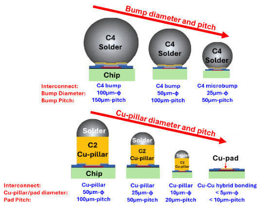
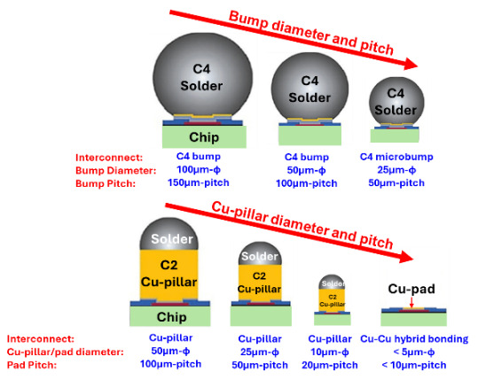
Cu-Cu hybrid bonding is one of the flip-chip bumpless assembly technologies. As shown in Figure 1, Cu-Cu hybrid bonding yields the highest density and performance, and finest pad and pitch of flip chip interconnects. With Cu-Cu hybrid bonding, it leads to a low profile, low thermal resistance, and low insertion loss 3D package. It is mostly suitable for silicon-to-silicon and silicon-to-glass assemblies. The assembly methods can be chip-on-chip (CoC), chip-on-wafer (CoW), wafer-on-wafer (WoW), chip-on-wafer-on-wafer (CoWoW), wafer-on-wafer-on-wafer (WoWoW), reconstructed wafer, direct transfer bonding, etc (Lau 2026; 2025b; 2025a; 2024b; 2023b; 2022). In this study, 21 different HVM or to be in HVM products and 13 new applications with Cu-Cu hybrid bonding will be briefly mentioned.
II. THE ORIGIN AND BRIEF FUNDAMENTAL OF HYBRID BONDING
Hybrid bonding (that combines a dielectric bond with a metal bond to form an interconnection) is known industry wide as low-temperature direct bond interconnect (DBI), which operates at room temperature and then anneals at, e.g., 150oC – 300oC. DBI was invented by the Research Triangle Institute (RTI) and patented it as ZiBond (a direct oxide to oxide bonding that involves wafer-to-wafer processing at room or low temperatures to initiate high bond strengths). Between 2000 and 2001, Fountain, Enguist, Tong, and several other colleagues, with their ZiBond (Tong, Fountain, et al. 2005; Tong et al. 2008), founded Ziptronic as a spin-out of RTI.
_of_hybrid_bonding.png)
Between 2003 and 2005, based on their ZiBond technology, Ziptronic combined the dielectric bond with embedded metal to simultaneously bond wafers and form the interconnects at low temperature (so-called DBI) (Tong, Enquist, et al. 2005; Tong et al. 2009). The breakthrough for Ziptronic DBI technology came in the spring of 2015 when Sony, already using its “Zibond” oxide to oxide bonding technology for their CMOS (complementary metal-oxide-semiconductor) image sensor (CIS), extended its license to include DBI. Today, the industry called DBI hybrid bonding.
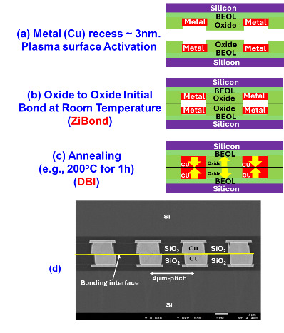
Figure 2 shows the key process steps for the hybrid bonding. First, controlling nanoscale topography is very important. The dielectric surface should be extremely flat and smooth before activation and bonding. Chemical–mechanical polishing (CMP) should achieve a very low dielectric roughness (< 0.5nm rms) and a certain recess (e.g., 3nm) of metal areas below the dielectric surface, as shown in Figure 2(a). Upon contact, the dry plasma-activated dielectric surfaces bond together instantaneously, as shown in Figure 2(b), at room temperature. Metal-to-metal bond occurs during batch annealing. The coefficient of thermal expansion of metals is typically far larger than dielectrics. The metal expands to fill the gap and then build up the internal pressure, as shown in Figure 2(c). It is under this internal pressure and annealing temperature that metal atoms diffuse across the interface, making a good metal-to-metal bond and, hence, electrical connection. In this case, the copper oxidation during bonding is minimized because the bonded oxide layer surrounding the copper interconnect protects the interconnect from oxidation in the annealing oven. The bonded oxide surface also hermetically seals the Cu interconnect during operation. Figure 2(d) shows an optimal Cu-Cu hybrid bonding with 4µm-pitch and 2µm-diameter pads.
_with_hybrid_bonding_(wow).png)
III. HIGH VOLUME MANUFACTURING (HVM) AND TO BE HVM PRODUCTS BY HYBRID BONDING
1. Sony’s CIS with WoW
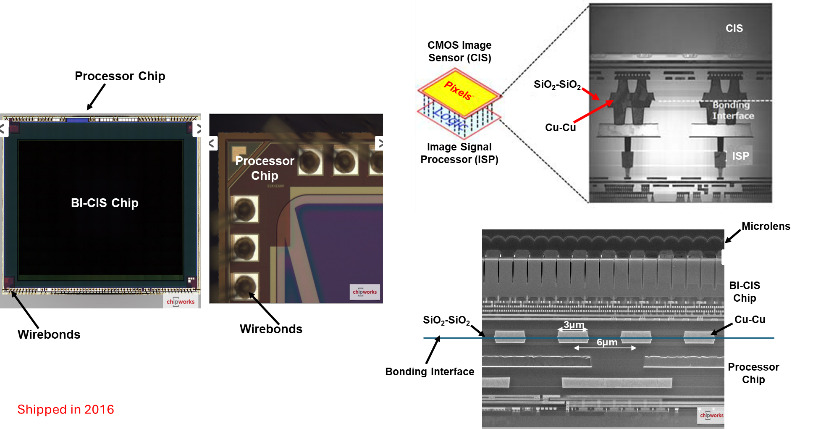
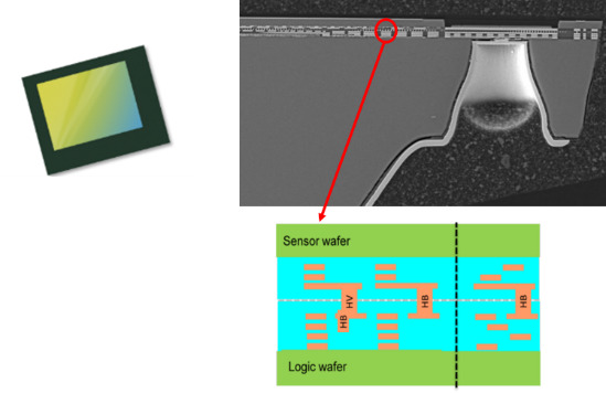
Sony is the first (n.d.-a) to use bumpless low-temperature Cu–Cu hybrid bonding in HVM. Sony produced the IMX260 backside-illuminated CMOS image sensor (BI-CIS) for the
Samsung Galaxy S7, which shipped in 2016. Top and cross section views of the IMX260 BI-CIS are shown in Figure 3. It can be seen that, unlike in Sony’s ISX014 stacked camera sensor, the through-silicon vias (TSVs) are eliminated, and the interconnects between the BI-CIS chip and the processor chip are achieved by Cu–Cu hybrid bonding. The pad size is 3µm and the pad pitch is 6µm. The signals are coming from the package substrate with wire bonds to the edges of the processor chip.
2. Sony’s CIS with WoWoW
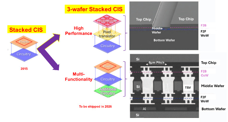
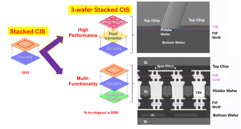
Figure 4 (Urata et al. 2024) shows the 3-wafer sacked CIS by Sony, which is for high-performance (photodiode-pixel-circuitry) and multi-functionality (pixel-circuitry-additional circuitry) applications. It can be seen that the top chip is bonded on the middle wafer with face-to-back (F2B) CoW (chip-on-wafer) bonding. Then, it is face-to-face (F2F) WoW (wafer-on-wafer) bonded with the middle wafer. Finally, the middle wafer with the top chip is bonded F2F (face-to-face) WoW with the bottom wafer. This 3-wafer sacked CIS is to be shipped in 2026.
3. OMNIVISON OX05B1S Sensor
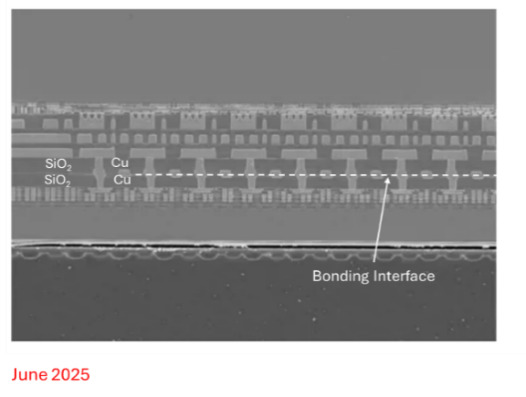
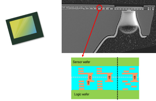
Figure 5 (n.d.-b) shows the OMNIVISON OX05B1S sensor. Unlike traditional sensors that use TSVs at the periphery, OMNIVISION OX05B1S uses direct copper-to-copper (Cu-Cu) connections. This “bumpless” hybrid bonding allows for a higher interconnect density and significantly smaller pixel sizes. Shipped in Q1 2023 for automotive in-cabin monitoring systems.
.png)
4. Samsung’s GM5 Imager
Samsung’s GM5 Imager (n.d.-c) is a 48-megapixel image sensor currently in mass production and widely utilized in flagship mobile devices in 2025. It has been notably integrated as the telephoto sensor in high-end devices like the Google Pixel 7 Pro (Figure 6) and Pixel 8 Pro.
-to-ccd_(back)_(cow).png)
5. AMD’s 3D V-Cache
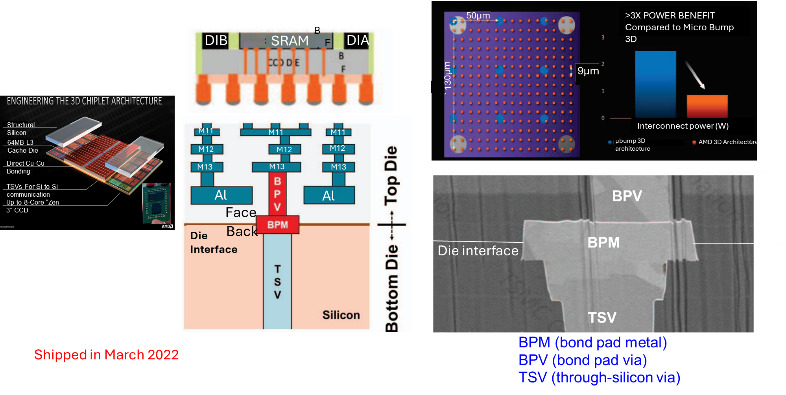
Figure 7 shows AMD’s 3-D V-Cache chiplet design and heterogeneous integration packaging (Agarwal et al. 2022). The key components of this structure are a bottom compute die, a top SRAM die, and structural dies to balance the structure and provide a thermal path for heat dissipation from the bottom compute die to the heat sink. The bottom die (81 mm2) is the “Zen 3” CPU, which is fabricated by TSMC’s 7-nm process technology. The top die (41 mm2) is the extended L3 die, which is also fabricated by TSMC’s 7-nm process technology. The bottom die with TSV is face-down with C4 bumps. The top die is also face-down, which is F2B Cu–Cu hybrid bonding (9 µm-pitch) to the bottom die. This product has been shipped to AMD’s favorite customers since March 2022.
_processor.png)
6. Graphcore’s Bow IPU Processor
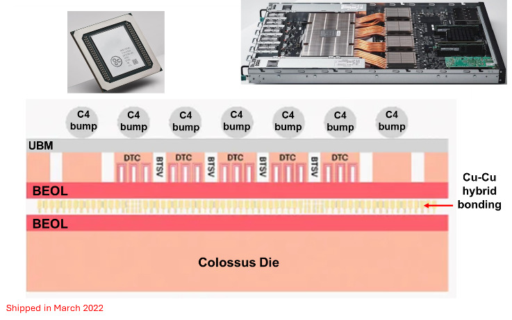
While IPU (intelligence processing unit) is the functional acronym for Graphcore’s specific class of AI-focused processors, “Bow” is the product’s codename (Moore 2022). IPU is a massively parallel processor designed from the ground up specifically to accelerate machine intelligence, artificial intelligence, and machine learning workloads. The Bow IPU is notable for being one of the world’s first processors to use 3D WoW hybrid bonding technology, which stacks a power delivery die (top) directly on top of the logic processor (bottom) to improve performance and efficiency (Figure 8). It was shipped in March 2022.
7. Jasminer’s ASIC Miner
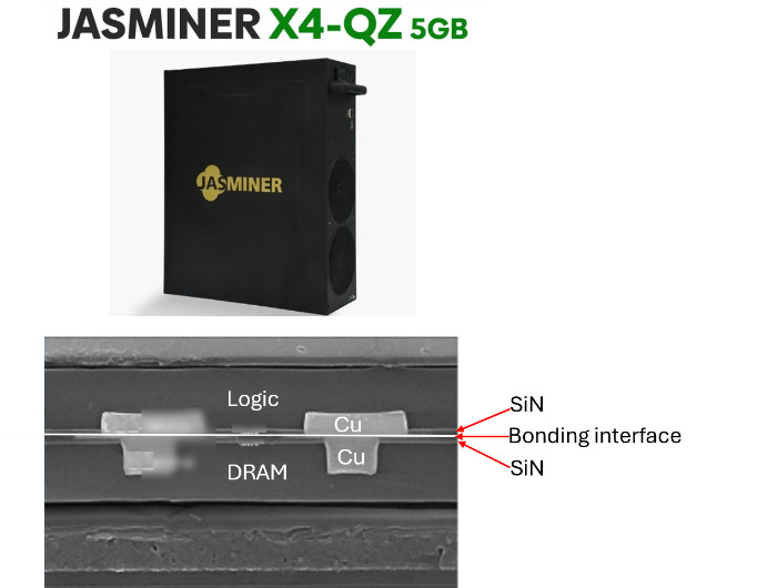
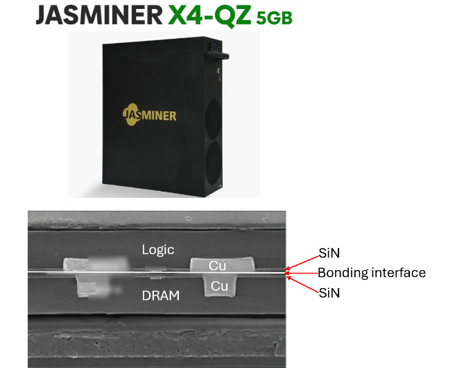
Jasminer’s ASIC Miner (n.d.-d) is designed for high-efficiency, quiet, and small-scale mining of Ethereum Classic (ETC) and other Ethash-based algorithms with Cu-Cu Hybrid Bonding (Figure 9). The Jasminer X4-Q was released in June 2022 (1040 MH/s at 480W), the Jasminer X4-Q-Z was launched in December 2022 (840 MH/s at 380W), and Jasminer X4-QZ was released in March 2023 (to further optimize efficiency for home mining environments).
8. AMD’s Compute and AI Chiplets
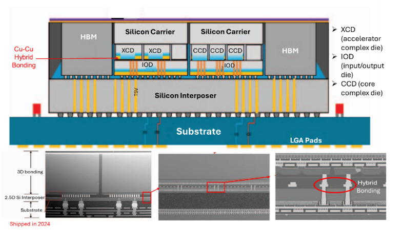
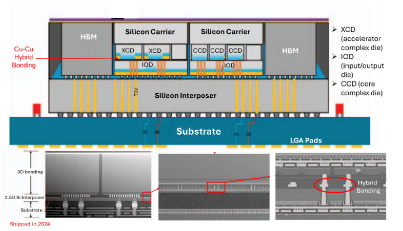
Figure 10 (Mandalapu et al. 2024) shows the AMD’s compute and AI chiplets which are stacked on top of the I/O and cache chiplets in their MI300 shipped in 2024. All the compute chips are built using TSMC’s N5 process. Neither the I/O functions nor the system’s cache memory benefit from N5, so AMD chose a less-expensive technology (N6) for those. Therefore, those two functions could then be built together on the same chiplet. MI300 stacks (with hybrid bonding the front-end optional part of Figures 10(a) and 10(b)) three CPU chiplets (called compute complex dies, or CCDs, in AMD’s lingo) and six accelerator complex dies (XCDs) on top of four input-output dies (IODs), on top of a piece of TSV-interposer that links them together to eight stacks of high-bandwidth DRAM (HBM) that ring the superchip. AMD also called this 3.5D IC integration.
9. Samsung’s X-Cube
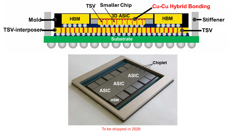
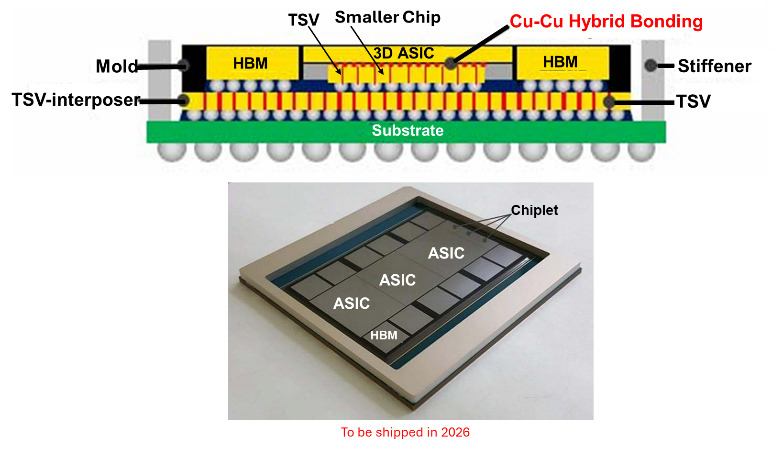
Figure 11 (Lee et al. 2023) shows the 3.5D IC integration or X-cube by Samsung, in which the ASIC is vertically stacked with two chips which are partitioned by its functional blocks. Each chip is stacked face-to-face interconnected with Cu-Cu hybrid bonding. Samsung Foundry showed a roadmap for 3.5D configurations in 2024, with projections for stacking 2nm and 4nm chiplets in 2025, and 1.4nm and 2nm chiplets in 2026.
10. Broadcom’s 3.5D XDSiP
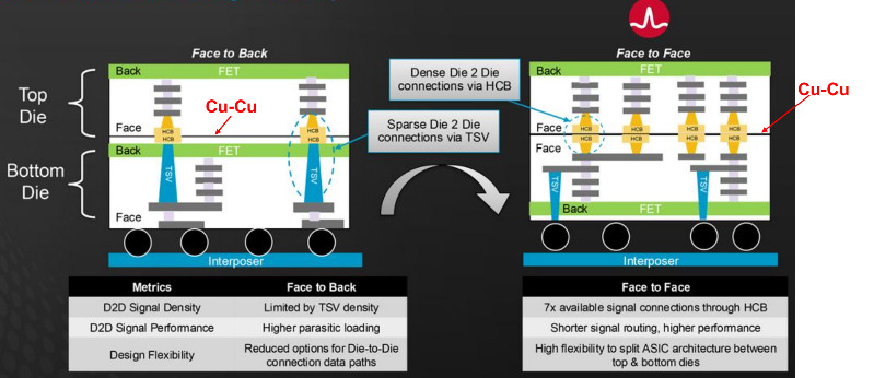
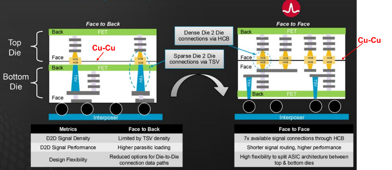
Broadcom (n.d.-e) has introduced its 3.5D eXtreme Dimension System in Package (3.5D XDSiP) platform for ultra-high performance processors driven by AI workloads. This platform uses TSMC’s CoWoS-L packaging technology that offers a maximum interposer size of approximately 5.5 times that of a reticle (about 858mm2), or 4719mm2 for compute chiplets, I/O chiplets, and up to 12 HBM3/HBM4 packages. To maximize performance, Broadcom suggests disaggregating the design of compute chiplets and stacking one logic chiplet on top of another in a face-to-face (F2F) manner using Cu-Cu hybrid bonding, Figure 12. It has been shipped to Fujitsu in February 2026.
11. Apple’s M5 Pro and M5 Max
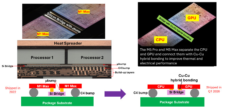
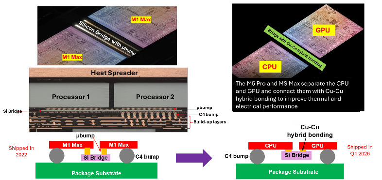
In 2022, Apple shipped their notebook computer with microbumps connecting the silicon bridge and the processors. Then, in Q1 of 2026, Apple shipped their new notebook computer MP5 Pro and MP5 Max with Cu-Cu hybrid bonding connecting the silicon bridge and the graphic processor unit (GPU) and central processor unit (CPU), Figure 13 (n.d.-f). It is for density, thermal and electrical performance, and low profile.
12. NVIDIA’s Rubin
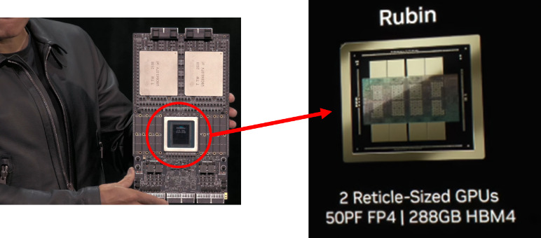
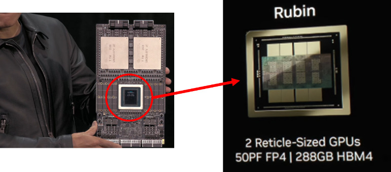
NVIDIA (n.d.-g) is scheduled to begin shipping the Rubin architecture, which utilizes hybrid bonding technology, in the second half of 2026, Figure 14. With hybrid bonding the NVIDIA Rubin allows for significantly higher interconnect density and better thermal management.
13. Intel’s Clearwater Forest
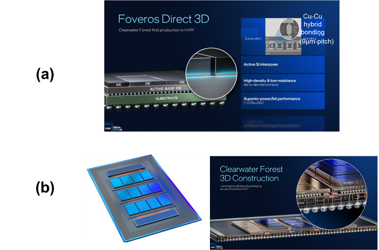
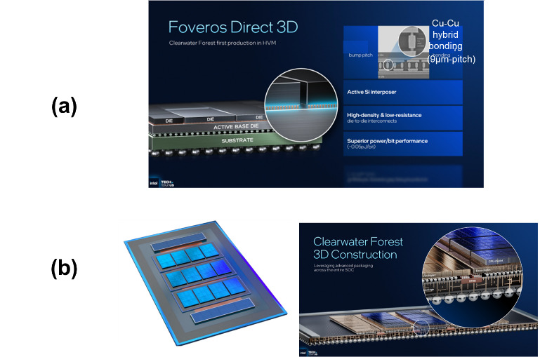
Intel’s Clearwater Forest (n.d.-h) is the first server-grade processor built on the Intel 18A process node and marks the debut of Intel’s Foveros Direct hybrid bonding (9µm-pitch) technology in high-volume production (to be shipped in the first half of 2026), Figure 15.
14. Samsung’s Hybrid Bonding for HBM
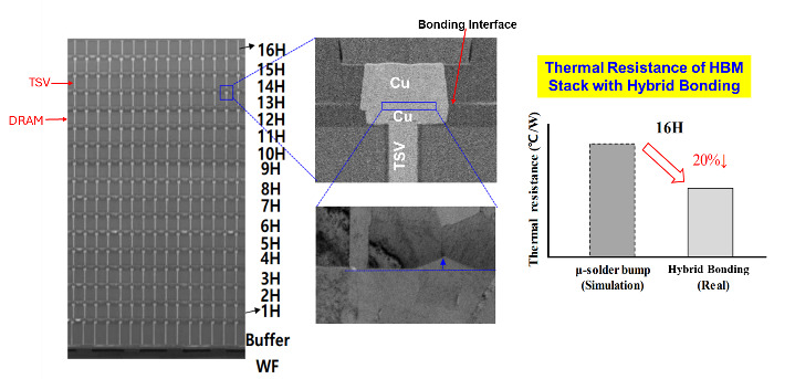
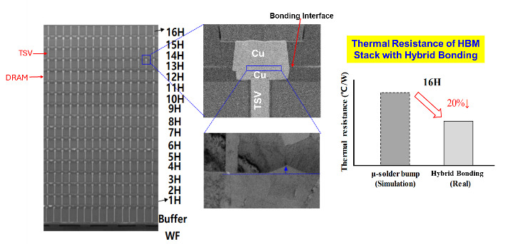
Figure 16 shows Samsung’s 16H multi–stack of dynamic random access memories (DRAMs) high bandwidth memory (HBM) with hybrid bonding technology (M. Kim et al. 2023; Taehwan et al. 2023; Hwang et al. 2023). The Cu-pad to Cu-pad is bonded with CoW and CoC methods. These methods are repeated to stack several core memory dies as CoC layers. After pre-bonding is completed by stacking the layers, the bond between oxides is strengthened by high-temperature annealing; the Cu pads of the top and bottom chips expand and meet, electrically connecting as Cu diffusion occurs. Because there are no gaps between the chips, the vertical thermal resistance of the 16H HBM with hybrid bonding is 20% lower than that by the flip chip with gaps for the µbumps and underfill. Samsung is planning to ship their HBM4 with hybrid bonding in early 2026 and HBM4E with hybrid bonding in mid-2026.
15. SK Hynix’s Hybrid Bonding for HBM
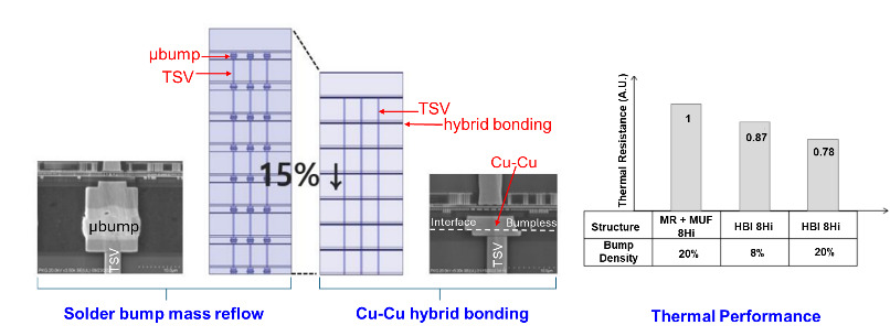
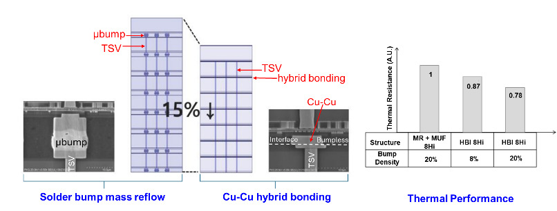
Figure 17 shows SK Hynix’s 8Hi multi-stack HBM with hybrid bonding (K. Kim et al. 2023). Compared with the solder bumped mass reflow method (MR+MUF), the thickness of the HBM package can be reduced by 15% with the Cu-Cu hybrid bonding method. It can also be seen that: (a) for the same bump (pad) density (20%), the thermal resistance of the hybrid bonding (8Hi) is 22% lower than that of the MR+MUF (8Hi), and (b) the thermal resistance of the hybrid bonding (8Hi) (with 8% pad density) is 13% lower than that of the MR+MUF (8Hi) (with 20% bump density). SK Hynix is planning to ship their HBM4E in 2027.
16. Micron’s Hybrid Bonding for HBM
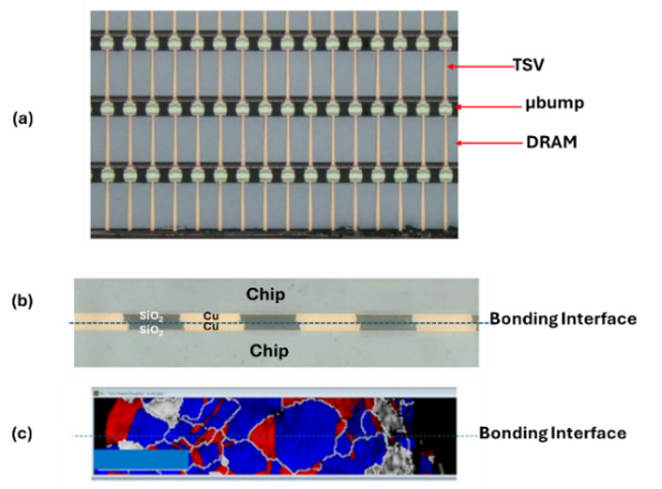
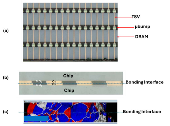
Figure 18(a) shows a conventional stacking of TSV-dies with µbumps solder reflow method for HBM (Zhou et al. 2023). The µbump pitch can go down to 20µm. However, with hybrid bonding, the Cu pad pitch can easily go down to 10µm and there is no bump, i.e., bumpless as shown in Figure 18(b). Figure 18(c) shows the electron backscatter diffraction (EBSD) across the bonding interface where two Cu pads are joined together.
Due to Cu-to-Cu diffusion, these two Cu pads become one with the Cu crystal growth occurring across the bonding interface. Micro is planning to ship their HBM with hybrid bonding in 2027.
17. YMTC’s 3D NAND Flash
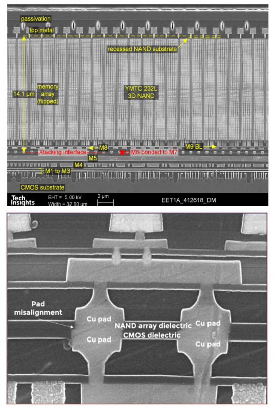
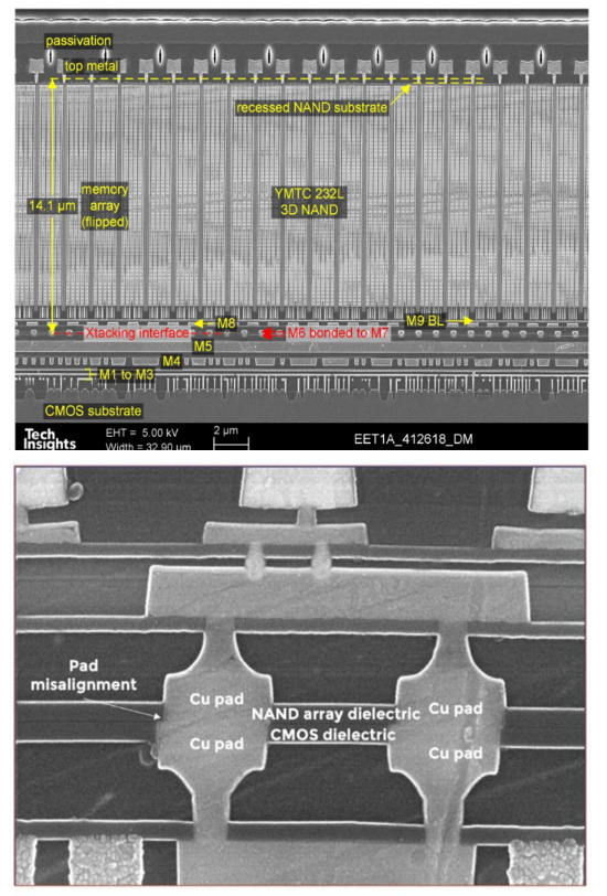
Yangtze Memory Technologies Co. (YMTC)'s 232 Layers 3D NAND flash memory by hybrid bonding technology shipped in 2023 is shown in Figure 19 (n.d.-i). It is known for its innovative Xtacking architecture. Unlike traditional 3D NAND, where memory cells and peripheral circuits are built on the same wafer, Xtacking manufactures them on two separate wafers and joins them using hybrid bonding.
_3d_nand_--_cmos_directly_bonded_to_array_(cba).png)
18. Kioxia-Western Digital’s 3D NAND Flash
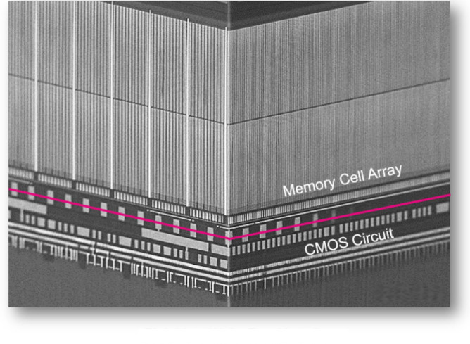
Figure 20 shows Kioxia-Western Digital’s BiCS8 (218-layer) 3D NAND – CMOS directly Bonded to Array (CBA) shipped in 2023 (n.d.-j). This approach is similar to YMTC’s Xtacking, where the logic circuitry (CMOS) and the memory cell array are manufactured on separate wafers and then hybrid bonded together.
_nand.png)
19. Samsung’s 10th-Gen (V10) NAND
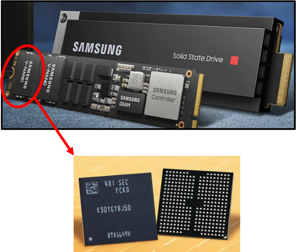
Samsung signed a licensing agreement with YMTC on their Xtacking architecture in early 2025. Samsung is currently scheduled to begin full-scale mass production of its 400+ layers 10th-generation (V10) V-NAND in October 2026, Figure 21 (n.d.-k).
_nand.png)
20. SK Hynix’s 10th-Gen (V10) NAND
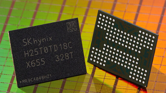
For 400+ layers counts, SK Hynix aims to complete development of the V10 pilot line in 2026, with full-scale mass production targeted for early 2027, Figure 22 (n.d.-l).
21. iPhone 18 to be sold in China
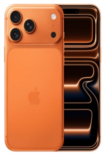
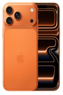
Apple is planning to use YMTC 3D NAND flash memory chips with the Xtacking architecture for iPhone 18 models to be sold (in September 2026) exclusively in the Chinese market, Figure 23 (n.d.-m). Apple’s iPhone market share in China was reported at approximately 29.48% as of March 2026.
IV. NEW APPLICATIONS WITH HYBID BONDING
1. Hybrid Bonding Bridge for Chiplets Heterogeneous Integration
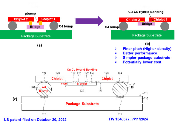
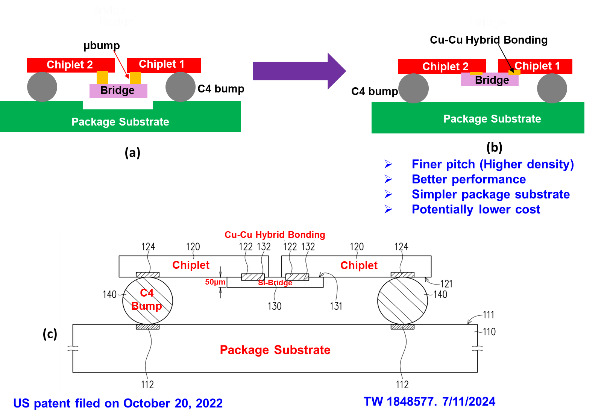
Unimicron proposed the use of Cu–Cu hybrid bonding for the bridge between chiplets in chiplet design and heterogeneous integration packaging, (Figure 24). The advantages of this structure are: (1) higher density, (2) finer pitch, (3) better performance, and (4) ordinary package substrate.
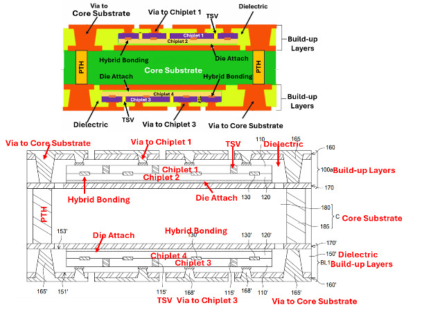
2. 3D Chiplets Embedded in Build-up Substrate with Hybrid Bonding
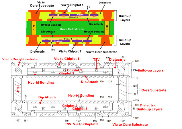
Embedding chips in build-up package substrates for high-density and high-performance applications is the trend for HPC. In order to embed more chips in the substrate, stacking up the chips in the build-up package substrate is one of the methods and hybrid bonding can keep the thickness of the stacking to the minimum. Figure 25 shows an example of embedded 3D chiplets with hybrid bonding in a build-up package substrate.
3. Package-on-Package - Chiplets Embedded in Fan-Out (RDL-First) EMC with Hybrid Bonding
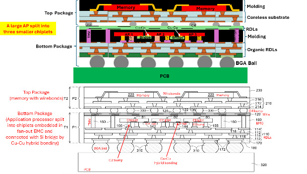
Package-on-package is a common packaging format for housing the application processor (bottom package) and the mobile memory (upper package). In order to save the semiconductor manufacturing cost, the large application processor is spelt into small chiplets (to have a higher yield).
_emc_with_hybrid_bonding.png)
Silicon bridges are used to connect the chiplets and Cu-Cu hybrid bonding is used between the bridges and processor chiplets, Figure 26.
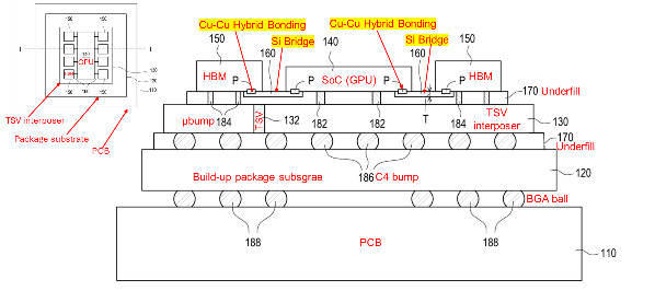
4. 2.5D IC Integration of SoC and HBMs with Bridge by Hybrid Bonding
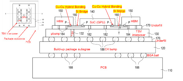
Today, the package of choice for HPC driven by AI is the chip-on-wafer-on-substrate (CoWoS). In order to enhance the performance, silicon bridges are used to connect the high bandwidth memory (HBM) and the system-on-chip (SoC) such as the graphic processor unit (GPU) by hybrid bonding as shown in Figure 27.
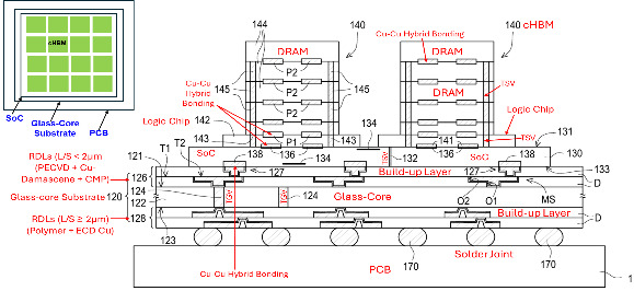
5. 3.3D IC Integration of cHBMs on Top of SoC on Glass Substrate
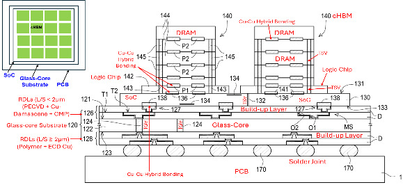
Figure 28 shows a new 3.3 IC integration structure. The interconnects between the DRAMs and logic base of the customized HBMs (cHBMs) are Cu-Cu hybrid bonded. The cHBMs are then (Cu-Cu hybrid bonding) directly attached to the top surface of the SoC. Finally, the SoC with cHBMs are Cu-Cu hybrid bonding directly attached to the top surface of a glass substrate.
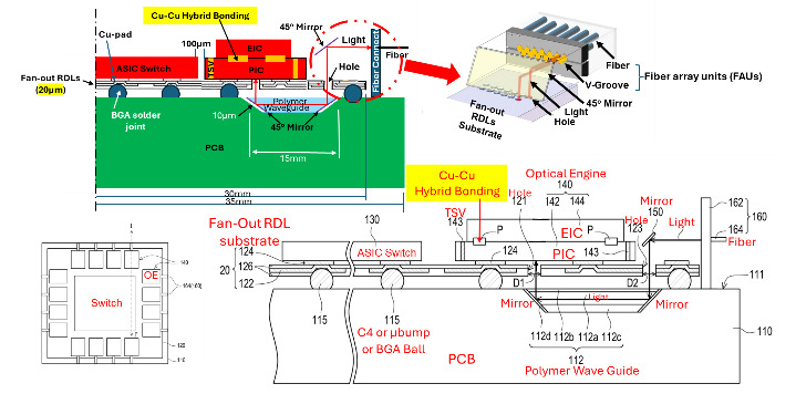
6. 3D Heterogeneous Integration of PIC and EIC with Hybrid Bonding on Fan-Out RDLs and Polymer Waveguides
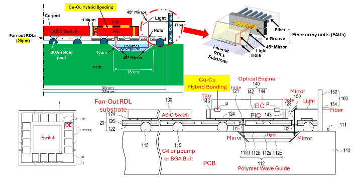
Figure 29 shows a co-packaged optics (CPO) system, in which the photonic integrated circuity (PIC) and electronic integrated circuity (EIC) are 3D stacked with hybrid bonding, and then they are side-by-side with a switch attached to a fan-out RDL CPO substrate with holes. The holes are used for lights to pass through. There are polymer waveguides with 45º mirrors at both of their ends that are semi-embedded in the PCB. The light from the external fiber through the V-groove hits the 45º physical mirror and then reflects and passes through the hole and hits one end of the 45º mirror of the polymer waveguide. The light travels along the polymer waveguide, hits the other end of the 45º mirror, and then reflects on the PIC. Finally, the photodiode (PD) in the PIC receives the light.
7. 3.5D Heterogeneous Integration of PIC and EIC with Hybrid Bonding on Organic Interposer with Polymer Waveguides
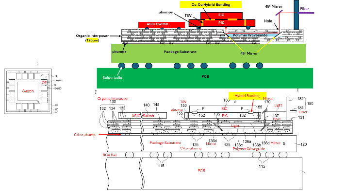
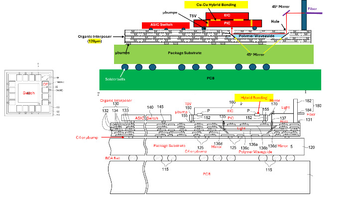
Figure 30 shows another CPO system. It can be seen that the PIC and EIC are stacked with hybrid bonding, and then they are side-by-side with the switch attached to an organic interposer with an embedded polymer waveguide with 45º mirrors at both ends. There are holes in the organic interposer. The CPO interposer is attached to a build-up package substrate, and then on a PCB.
8. 3.5D Heterogeneous Integration of PIC and EIC and Switch with Si Bridge by Hybrid Bonding
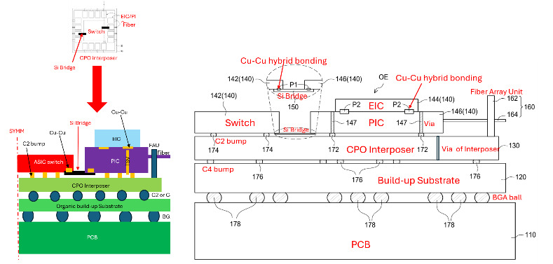
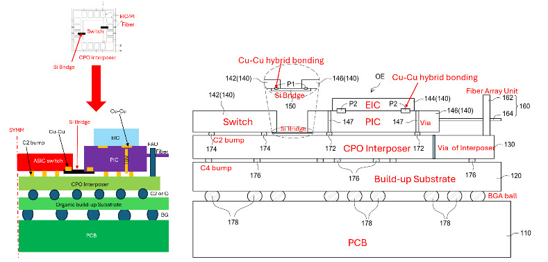
Figure 31 shows another CPO system, where the optical engines (PIC and EIC) are stacked with hybrid bonding. In order to enhance the performance, the switch is connected to the PIC with hybrid bonding. The switch and the optical engines are side-by-side on a CPO interposer and then on a package substrate.
9. 3D Heterogeneous Integration of PIC and EIC with Glass Interposer and Hybrid Bonding
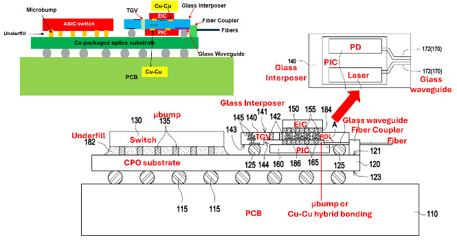
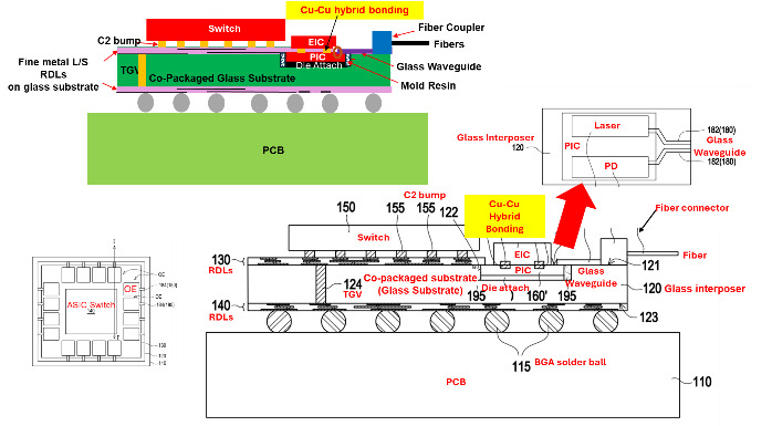
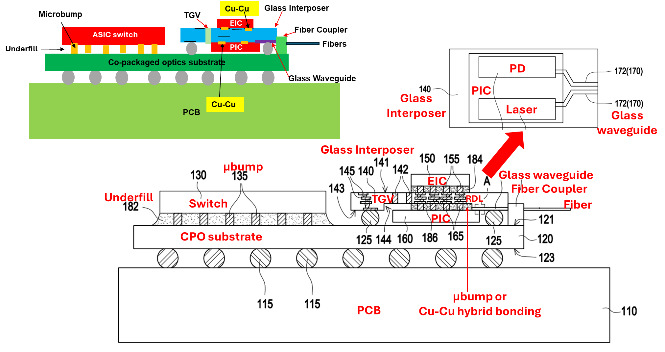
Figure 32 shows another CPO system with a through glass via (TGV) interposer. The PIC and EIC are 3D-stacked through a TGV interposer with Cu-Cu hybrid bonding. The PIC and EIC are side-by-side with the switch attached to a build-up package substrate. The package substrate is then attached to the PCB. The glass waveguide on the glass interposer receives the light from the external fiber and sends the light to the PD of the PIC.
10. 3D Heterogeneous Integration of EIC and PIC by Hybrid Bonding with the PIC Embedded in a Co-Packaged Glass Substrate
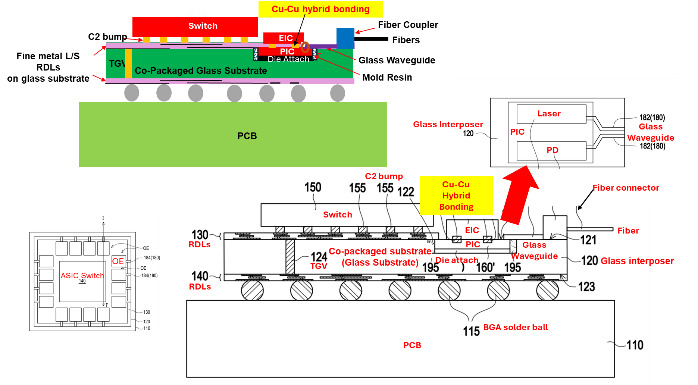
Figure 33 shows another CPO structure with a glass-core build-up package substrate. There is a cavity on the CPO glass-core substrate. The PIC and EIC are 3D-stacked with hybrid bonding, and the PIC is semi embedded in the cavity of the substrate. The switch and the PIC/EIC stack are side by-side attached to the CPO substrate. Compared to the CPO structure shown in Figure 32, this CPO structure has better performance but has a higher cost.
11. 3D Heterogeneous Integration of EIC and PIC by Hybrid Bonding with Silicon Photonics
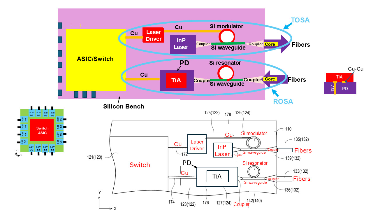
Figure 34 shows a 3D heterogeneous integration of EIC and PIC by hybrid bonding with silicon photonics. CPO with silicon photonics is defined as the silicon InP laser, silicon Germanium photodetector, silicon waveguides, silicon modulators/resonators, couplers, etc. are fabricated on a silicon wafer with CMOS technology. These elements (on a CPO silicon substrate or interposer) enable high-speed, high-bandwidth, energy-efficient optical interconnects that overcome the physical limitations of traditional copper wiring in high-performance computing and data centers driven by artificial intelligence.
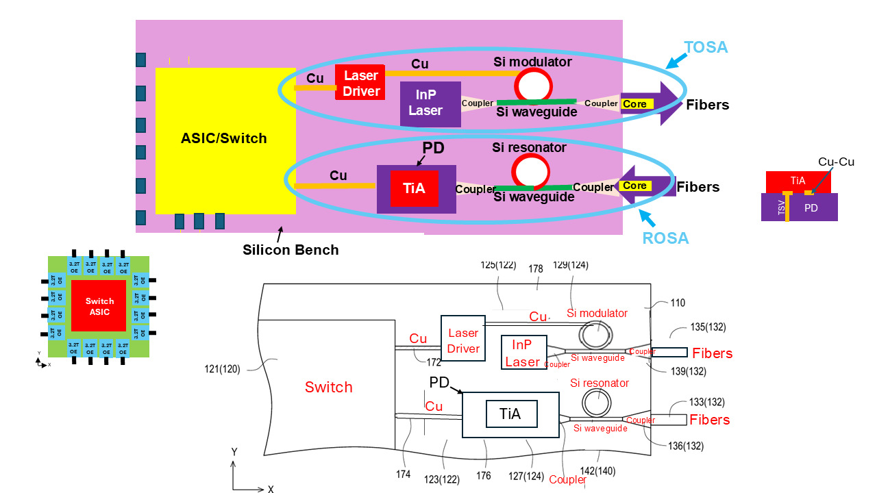
For the receiver optical subassembly (ROSA) of a CPO with silicon photonics, the light from a fiber coupled to the silicon waveguide which confines the light. Then the silicon resonator (with Germanium) changes light to optical signal. Finaly, the photodetector (PD), usually made by Germanium, of the PIC changes the optical signals to electrical signals, which are then amplified by the transimpedance amplifier (TIA) of the EIC before connected to the switch. The TiA is stacked on the PD by Cu-Cu hybrid bonding.
For the transmitter optical subassembly (TOSA) of a COP with silicon photonics, the silicon modulator injects or depletes the electrons and holes (charge carriers) of the electrical signal (voltage) of the switch in the silicon waveguide. While the silicon modulator processes the data, the laser driver of the EIC is the power and control engine for the light source itself. It provides stable power supply and signal amplification before the light is shot out from the laser (usually made by InP) of the PIC to the fiber.
12. Thermal Management of 2.5D IC Integration with Hybrid Bonding and TSV Interposer with Microchannels
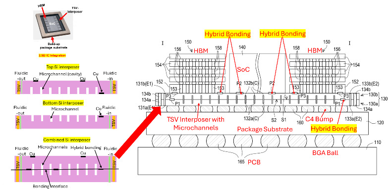
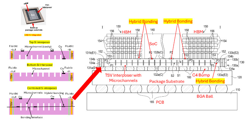
Figure 35 shows a 2.5D IC integration system with hybrid bonding and TSV-interposer with microchannels. In the figure, the TSV-interposer is fabricated with two silicon wafers and etched into microchannels. Then these two wafers are dielectric-to-dielectric and metal-to-metal hybrid bonded together which forms a totally shielded boundary for the fluid. The chiplets are also hybrid bonded on the thermal enhanced TSV-interposer.
13. Thermal Management of 2.5D IC Integration with Microchannels and Cu-Cu Hybrid Bonding
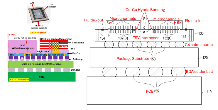
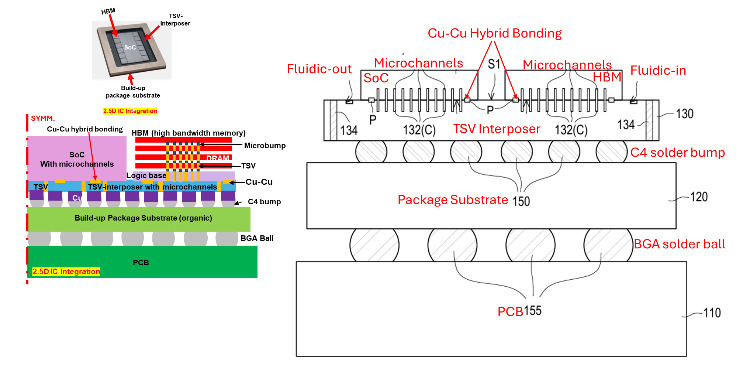
Figure 36 shows a thermal management of 2.5D IC integration with microchannels and Cu-Cu hybrid bonding. The chiplets and the TSV interposer are etched with microchannels, and dielectric-to-dielectric and metal-to-metal hybrid bonded together. The thermal performance of this case is better than that of Figure 34 but with a higher cost.
V. SUMMARY
Some important results and recommendations are summarized as follows.
-
The origin and brief fundamentals of hybrid bonding have been provided.
-
Hybrid bonding is an old flip-chip assembly technology. It has been in HVM since 2016. For example, from the CIS for smartphones by Sony, Samsung, etc. and for automobiles by OMNIVISON, etc. memory-on-logic and logic-on I/O for HPC by Jasminer, Samsung, AMD, Graphcore, Broadcom, NVIDIA (second half of 2026), Intel (first half of 2026), etc., HBM by Samsung (2026), SK Hynix (2026 or 2027), Micron (2027), etc., GPU-bridge-CPU for notebooks by Apple, to 3D NAND flash by YMTC, Kioxia-Western Digital. Samsung (to be shipped in Q4 2026), SK Hynix (to be shipped in early 2027), Apple iPhones (September 2026 in China market), etc.
-
Thirteen new applications with hybrid bonding have been proposed.
-
In order to enhance performance and reduce package size, 3.5D IC integration with hybrid bonding is strongly recommended.
-
As of today, there are not many articles published on the quality and reliability (such as the thermal cycling, thermal shock, mechanical vibration, mechanical shock, high temperature storage, highly accelerated temperature, and highly accelerated moisture resistance) of Cu–Cu hybrid bonding. For the hybrid bonding to be more popular, these quality and reliability data are desperately needed.
-
Thermal management of Cu–Cu hybrid bonding (stacking chips) will be an important topic.
-
Also, we would like to know the answers to the following questions: a) what is the effect of Cu–Cu bonding misalignment on the quality and reliability of Cu–Cu hybrid bonding interconnect? and b) what is the effect of bonding interface void (size, location, and propagation) on the quality and reliability of Cu–Cu hybrid bonding interconnect?