
1. Introduction
In the past, the performance of semiconductor products has been driven by Moore’s law – smaller feature size leads to more transistors. However, for HPC and data centers in AI era, the performance is not only driven by purely Moore’s law (smaller process nodes) but also by (a) how the chips are partitioned into chiplets, (b) how the chips are split into chiplets, (c) how the chiplets are stacked, (d) how the chiplets are interconnected, (e) how the chiplets are cooled, and (f) how the chiplets are packaged. The methods, among others, are: (a) chiplets heterogeneous integration (Lau 2019), (b) bridges connecting chiplets (Lau 2021), (c) Cu-Cu hybrid bonding (Lau 2023), (d) panel-level packaging (Lau 2024), (e) glass packaging (Lau and Fan 2025), (f) co-packaged optics with Si/Glass photonics (Lau and Chiang 2026), (g) innovative materials and characterizations (Lau 2019; 2021; 2023; 2024; Lau and Fan 2025; Lau and Chiang 2026), (h) superior quality and reliability (Lau 2019; 2021; 2023; 2024; Lau and Fan 2025; Lau and Chiang 2026), (i) process integration within existing manufacturing environments (Lau 2019; 2021; 2023; 2024; Lau and Fan 2025; Lau and Chiang 2026), and (j) superior thermal management (Lau and Fan 2025). Glass packaging is the focus of this study.
From 2007 to 2020, there were only a few organizations working on glass packaging (Bhatt et al. 2007; Cui et al. 2007; Brusberg, Schroder, Topper, Arndt-Staufenbiel, et al. 2009; Brusberg, Schroder, Topper, and Reichl 2009; Schroder et al. 2010; Topper et al. 2010; Sukumaran et al. 2010; Tummala et al. 2011; Sukumaran et al. 2012; McCann 2014; Ostholt et al. 2014; Bowrothu et al. 2018; Hwangbo et al. 2018; Ravichandran et al. 2020; Wong et al. 2020; Ali et al. 2020). However, in the past few years, because of the HPC driven by AI, glass packaging has been attracting lots of traction (Erdogan et al. 2021; Sivapurapu et al. 2021; Huang and Swaminathan 2021; Okoro et al. 2021; Pan et al. 2021; Jayaram et al. 2022; Pan et al. 2022; Jia et al. 2022; Ravichandran et al. 2022; Kim et al. 2023; Yeary et al. 2023; Li et al. 2023; Kathaperumal et al. 2024; Molina-Mangual et al. 2024; Kim et al. 2024; Brusberg et al. 2024; Yang et al. 2024; Xing et al. 2025b; Chen et al. 2025a; Sunohara et al. 2025a; S. et al. 2025; Sunohara et al. 2025b; Mizuno 2025; Wei et al. 2025; Jiang et al. 2025; Fujimoto et al. 2025; Khorasani et al. 2025; Kim et al. 2025; Tanaka et al. 2025; Morikawa et al. 2025; Yang et al. 2025; Ikumoto et al. 2025; King et al. 2025; Brusberg et al. 2025; Otsu et al. 2025; Kanungo et al. 2025; Lau et al. 2025; Pietambaram et al. 2026; Yin et al. 2026; Hu et al. 2026; Kim et al. 2026; Fujimoto et al. 2026; Sohara et al. 2026; Lee 2026; Tanwar et al. 2026; Panse 2026; Otsu 2026; Kobayashi et al. 2026; Kawasak et al. 2026; Ambrosius et al. 2014; Xing et al. 2025a; Chen et al. 2025b; “Intel Unveils Industry-Leading Glass Substrates” 2023; n.d.).
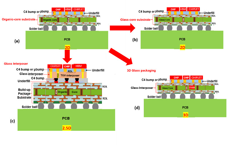
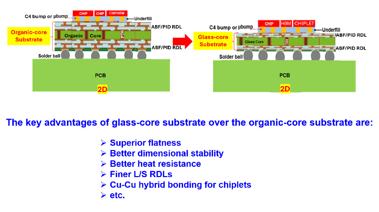
Some of the glass packaging is shown in Figure 1. The organic-core build-up package substrate, Figure 1(a), has been replaced by the glass-core build-up package substrate, Figure 1(b). Also, the traditional through silicon via (TSV) interposer (Lau 2013) has been replaced with the through glass via (TGV) interposer, Figure 1(c) - a 2.5D IC integration. A TGV glass-core interposer that is supporting chips is also supported by an organic-core substrate as shown in Figure 1(c). Finally, a chip is embedded in the glass-core build-up package substrate, i.e., a 3D IC integration, Figure 1(d).
_organic-core_substrate._(b)_glass-core_substrate._(c)_glass_(tgv)_int.png)
2. Through-glass Vias (TGV) and Redistribution-Layers (RDLs)
2.1. TGV
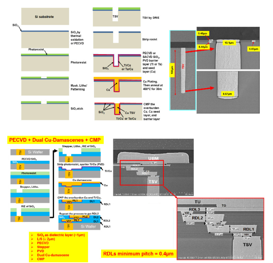
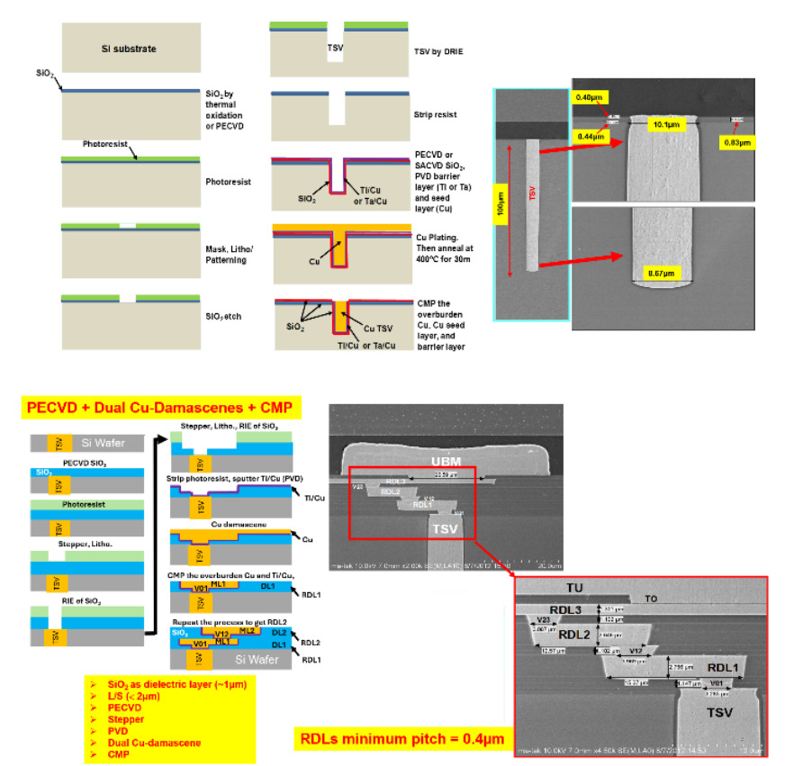
The fabrication process of TGV is very different from that of TSV. Most of the TSVs are fabricated by the deep reactive-ion etching (DRIE) (Lau and Fan 2025) as shown in the top of Figure 2. However, today most of the TGVs are fabricated by laser drilling such as the laser induced deep etching (LIDE) developed by LPKF Laser & Electronics AG in 2017 (Ambrosius et al. 2014). The most common used glass materials are the SCHOTT AF 32 alkali-free flat glass and the CORNING HPFS 7980 high purity non crystalline fused silica glass. Both materials have low CTE, which are close to that of silicon.
_tgv_process_flow._(b)_sem_image_of_a_tgv._(c)_etch_solution_mechanism.png)
_tgv_sidewall_metallization._(b)_cu_plating._(c)_an_image_of_cu-filled_tgv.png)
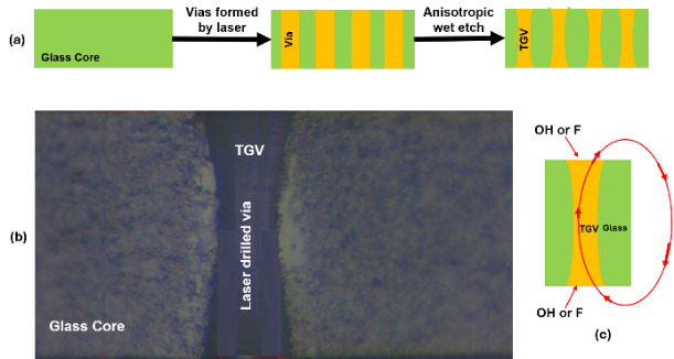
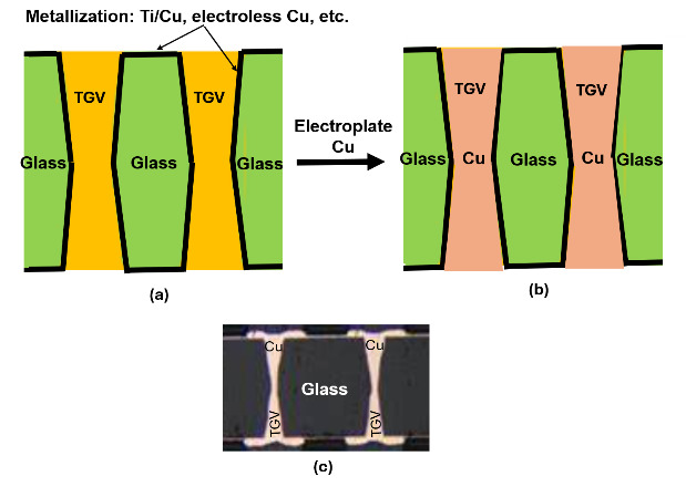
The process flow for fabricating the TGV is shown in Figure 3(a). It can be seen that the vias are formed by high-speed laser and the modified area of the glass are removed by anisotropic wet chemical etching, e.g., hydrofluoric acid (HF) or sodium hydroxide (NaOH). Figure 3(b) shows a typical TGV. There is a taper angle of the TGV. This is due to the rate of the circulation and temperature of the etching solution, and the concentration difference of the etching solution. This process results in making the outer ionizer move inward and be replenished as shown in Figure 3(c). The higher the etching rate the larger the taper angle. It is followed by the metallization of the seed layer, which can be materials such as Ti/Cu, electroless Cu, etc. as shown in Figure 4(a). Then, electroplate the Cu to fill the via as shown in Figure 4(b), Figure 4(c) shows an SEM image of the Cu-filled TGV. Table 1 shows the summary of the process compression between the TSV and TGV.
2.2. RDLs
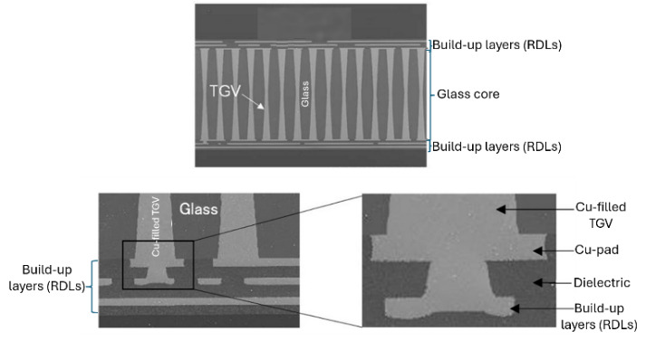
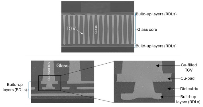
Depending on the linewidth (L) and spacing (S) of the RDLs, there are at least three methods in fabricating the RDLs. One method is for the conventional RDLs (linewidth (L), and spacing (S) are between 2µm and 10µm with polymers such as photo imageable dielectric (PID) or Ajinomoto build-up film (ABF) for the dielectric layer and electrochemical deposition (ECD) Cu for the conductor layer. The polymer is spin-coated on the silicon wafer (or slit-coated on the glass panel). The other method is for L/S < 2µm RDLs (Lau and Chiang 2026). In this case, the RDLs are fabricated with the 64nm process technology. The dielectric layers (SiO2) are fabricated by plasma enhanced chemical vapor deposition (PECVD). The metal layers are fabricated by dual Cu-damascene and chemical-mechanical polishing (CMP). This method is used for most RDLs of TSV-interposer in HPC and data centers driven by AI and the minimum pitch of the RDLs is 0.4µm as shown in the bottom of Figure 2. The third method is for L/S ≥ 10/15µm, the dielectric material can be resin, and the conventional sequential build-up process is adequate. Figure 5 shows the SEM images of some TGVs and RDLs made by the second method (L/S ≥ 2µm). The key challenges of fine linewidth and spacing RDLs are their thickness uniformity and yield due to warpage.
3. Panel-Level Packaging vs. Wafer-Layer Packaging
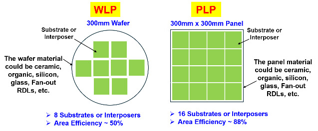
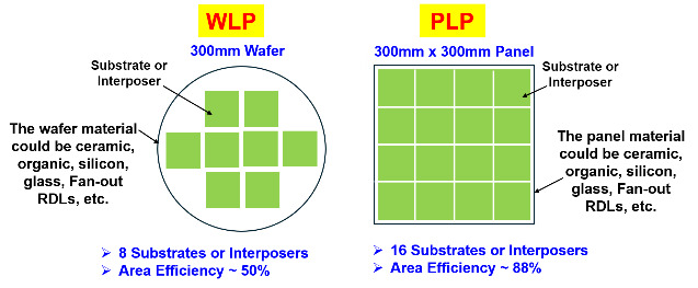
Wafer-level packaging (WLP) has been in high-volume production for more than 25 years. In the past few years, panel-level packaging (PLP) has been gaining a lot of traction, e.g. (Lau and Chiang 2026),. PLP has better area efficiency (which leads to lower costs) compared to WLP as is obviously shown in Figure 6, especially for larger size of substrate or interposer. For both WLP and PLP, the materials of the substrate or interposer could be ceramic, organic, silicon, glass, fan-out RDLs, etc.
4. Intel’s Glass Packaging
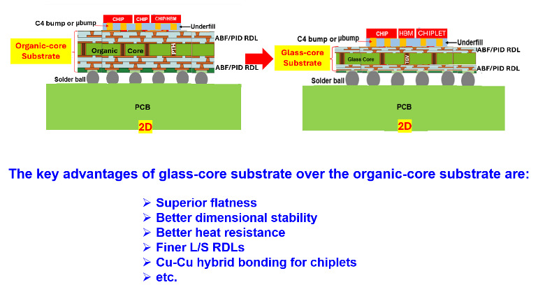
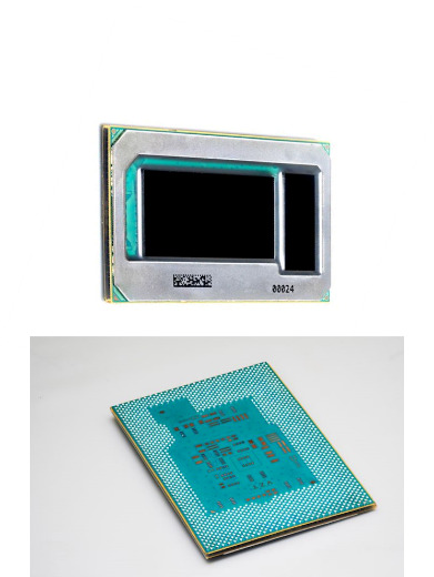
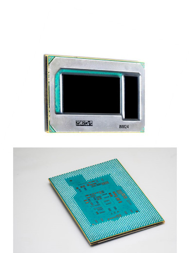
On September 18, 2023, Intel announced that they have been spending more than one billion dollars on research and development and are on the path to delivering one trillion transistors on a package by 2030 and its ongoing innovation in advanced packaging including glass substrates will help achieve this goal. Figure 7 shows Intel’s glass packaging. It can be seen that the popular organic-core substrate is replaced by the glass-core substrate for their one trillion transistors application. One of their fully functional test chips is shown in Figure 8. There are three layers of RDLs, and the TGVs are on a 75µm pitch.
During July 2025, Intel stopped all their in-housing glass manufacturing activities and started licensing its extensive glass patents (> 700) to their suppliers. On July 28., 2026, intel signed a memorandum of understanding with Lens International (HK) limited on how to fabricate crack-free through-glass via.
5. TSMC’s Glass Packaging
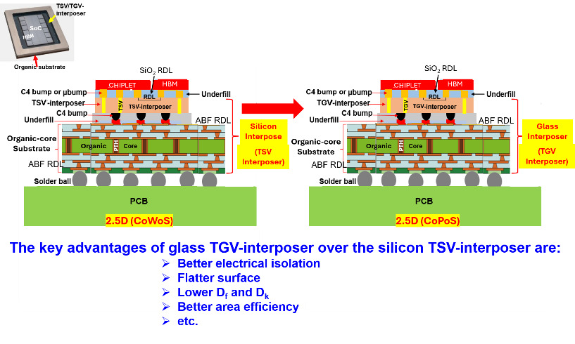
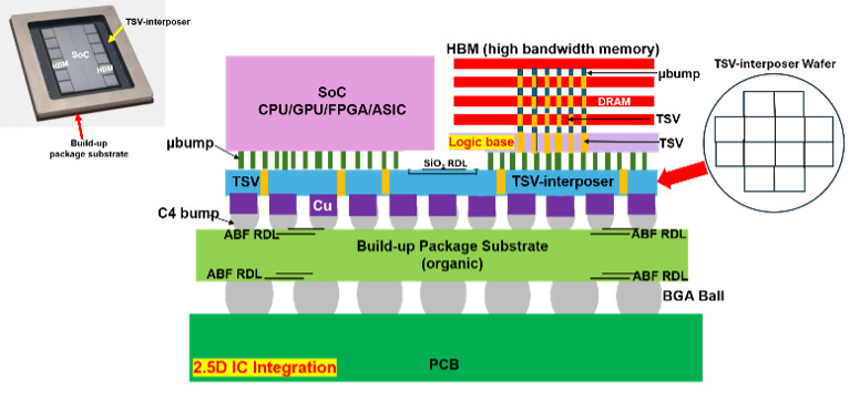
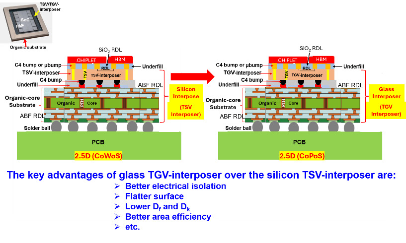
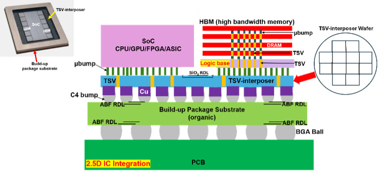
During the TSMC 2025 North America Technology Symposium (April 23), the company announced its chip on panel on substrate (CoPoS) technology and is scheduled to be shipped in Q1 of 2029, which is competing with its very popular chip on wafer on substrate (CoWoS) technology, Figures (9) and 10. Figure 10 schematically shows the CoWoS package, which is the package of choice for HPC data centers driven by AI today. It can be seen that the system-on-a-chip (SoC) and the high-bandwidth memories (HBMs) are supported by a TSV interposer with SiO2 RDLs (L/S = 0.2µmmin) on its top side that are fabricated on a 300mm silicon wafer. Because of the gag order of CoPoS imposed by TSMC to its suppliers, the real package structure of CoPoS can only be known until the tear-down of the first product.
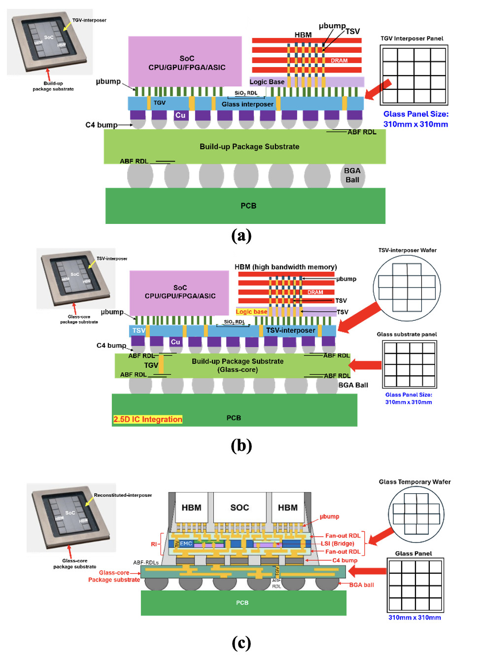
In this study, we will talk about three possibilities of the CoPoS package structure. Figure 11 schematically shows three options of the CoPoS package. For option one, CoPoS-v1 (Figure 11(a)), the TSV-interposer in CoWoS is replaced by a TGV-interposer which is fabricated on a 310mm x 310mm glass panel with SiO2 RDLs (L/S = 0.2µmmin) on its top side. Then the TGV-interposer is attached to an organic substrate with ABF RDLs on its top and bottom sides, Finally, the whole package is attached to PCB. For option two, CoPoS-v2, (Figure 11(b)), which is the same as Figure 10 (CoWoS), except the organic-core substrate is replaced by a glass-core substrate with ABF RDLs (L/S ≥ 2µm) on its top and bottom sides, which is fabricated by a 310mm x 310mm glass panel. For option three, CoPoS-v3, (Figure 11(c)), the TSV-interposer in Figure 10 (CoWoS) is replaced by the Reconstituted-Interposer (Si bridges embedded in panel fan-out epoxy molding compound with RDLs) so called CoWoS-L. The reconstituted interposer is fabricated by the fan-out packaging method on a temporary glass wafer. Instead of the organic-core package substrate in CoWoS, a glass-core package substrate with ABF RDLs (L/S ≥ 2µm) on its both sides is used and fabricated on a 310mm x 310mm glass panel. It is obvious that CoPoS-v1 has the best performance with the highest cost and challenges while CoPoS-v3 has the lowest performance but with the lowest cost and challenges.
TSMC has planned to establish its first CoPoS pilot line at Chiayi in 2026 with mass production facilities located at its P4 and P5 plants in AP7, Chiayi. Mass production is expected to begin as early as the first half of 2029. The technical challenges of CoPoS are RDL thickness uniformity and yield loss due to large panel warpage.
The first wave of equipment supply chains has been largely finalized, with specifications and order volume confirmed. The international companies involve KLA, TEL, Screen, Applied Materials, and Disco. The Taiwanese companies are Innolux, Sin-Yun, Hung-Soo, Chung Hwa, Chromium, Chih-Sheng, and Da-Long.
_copos-v1._(b)_cowos-v2._(c)_cowos-v3.png)
_flip-chip_on_an_organic-core_substrate._(b)_flip-chip_on_a_glass-core_substrate.png)
6. Status of Panel Size for HPC Driven by AI
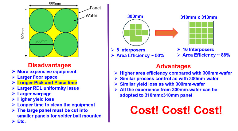
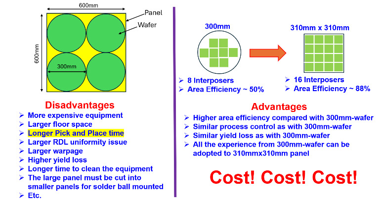
Figure 15 shows a comparison between the 600mm x 600m panel and 310mm x 310mm panel. It can be seen that the disadvantages of the 600mm x 600mm panel are more expensive equipment, larger floor space, longer pick and place time, larger RDL thickness uniformity issue, larger warpage, higher yield loss, longer time to clean the equipment, the large panel must be cut into smaller panels for solder ball mounting, etc. While the advantages of the 310mm x 310mm panel are higher area efficiency compared to 300mm-wafer, similar process control as with 300-mm wafer, similar yield loss as with the 300-mm wafer, most successful experience from 300mm-wafer can be adopted to 310m x 310mm panel, etc.
Take the pick and place as an example, Table 2 shows the throughput and processing time comparison between the 600mm x 600mm and the 300mm-wafer. With different chip sizes, the pick and place time of the 600mm x 600mm panel is a few times the 300-mm wafer. If the next step is for compression molding, i.e., epoxy flow (3 minutes) + compression (10 minutes), then the compression molding equipment must be idle for a very long time. The compression molding equipment idle time (%) is shown in Table 3. To have the manufacturing line balanced, the required 600mm x 600mm panel cluster sizes for no idling are shown in Table 3. This is just one of the hiding facts about the 600mm x 600m panel.
In March 2026, while ASE originally planned for a 600mm x 600mm panel line, it scaled back to 310mm x 310mm to align with TSMC’s panel size. ASE aims to have a fully automated 310mm x 310mm production line operational for pilot production by the end of 2026. On May 26, 2026, ASE formally announced the 310mm x 310mm panel size by the CEO of ASE at IEEE/ECTC 2026.
Due to alignment between currently leading organizations such as TSMC and ASE on 310mm x 310mm, the market is poised to shift from experimentation to volume production. Standardizing this panel size 310mm x 310mm is expected to help the entire semiconductor ecosystem scale AI chip packaging more reliably by providing a common platform for testing and manufacturing.
The 310mm × 310 mm format strikes a critical balance for HPC and data centers in AI era: it is large enough to capture the area efficiency (cost) and small enough to maintain the processing control (yield). Also, most of the successful experiences from 300mm wafer can be transferred to 310mm x 310mm panel.
7. Coefficient of Thermal Expansion of Glass
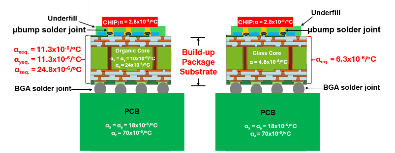
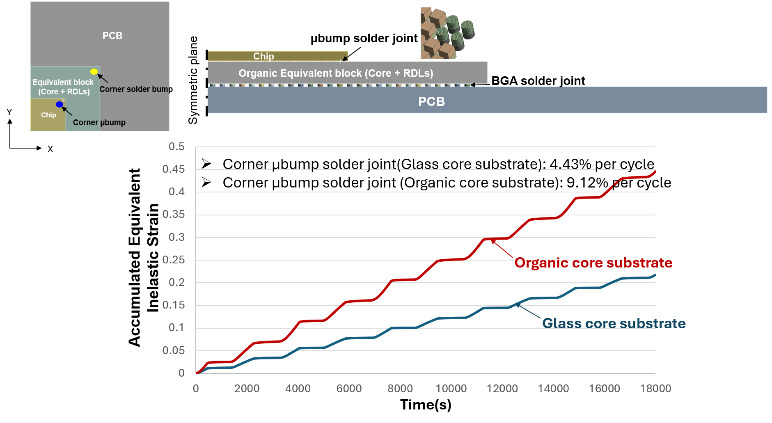
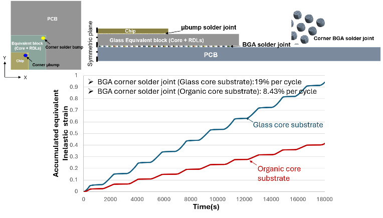
Figure 12 shows a flip chip on an organic-core substrate assembly, Figure 12(a), and on a glass-core substrate assembly, Figure 12(b). Currently in the industry, in order to match the CTE of the silicon chip (2.5x10⁻⁶/oC), the glass CTE is made to be as close as that of the silicon chip. In [78. 79], we have demonstrated that it is not a good idea for the ball grid array (BGA) solder joint reliability on the printed circuit board (PCB).
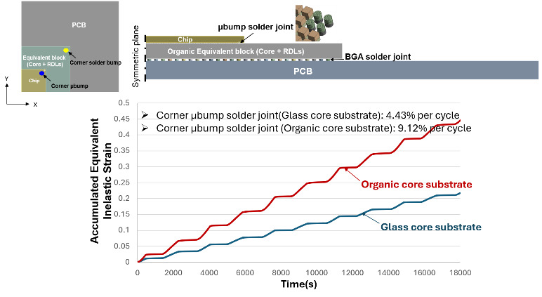
Figure 13 shows the accumulated equivalent inelastic strain time-history in the corner µbump solder joint between the chip and the organic-core substrate or the glass-core substrate. The accumulated equivalent inelastic strain in the corner µbump solder joint is 4.4% per cycle with the glass-core substrate and 9.12% per cycle with the organic-core substrate. It should be noted that there is underfill to protect the µbump solder joint on the glass-core or organic-core substrate so there is not any µbump solder joint reliability issue.
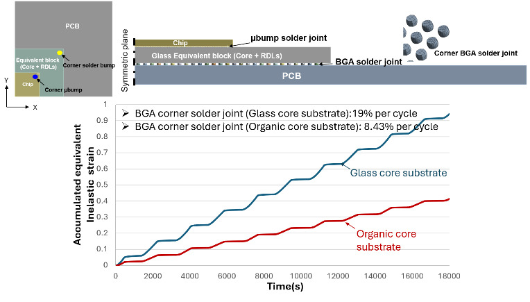
Figure 14 shows the accumulated equivalent inelastic strain time-history in the corner BGA solder joint between the organic-core substrate or the glass-core substrate and the PCB. The accumulated equivalent inelastic strain in the corner BGA solder joint is 19% per cycle with the glass-core substrate and 8.43% per cycle with the organic-core substrate. It should be noted that there is no underfilled to protect the BGA solder joint on the PCB, so there could be a BGA solder joint reliability issue. The comparison of the inelastic strain in the corner µbump solder joint and the corner BGA solder joint for glass-core substrate and organic-core substrate is shown in Table 4.
_tsv-interposer__(b)_tgv-interposer__and_(c)_organic-interposer.png)
8. Summary and Recommendations
Some important results and recommendations are summarized as follows.
-
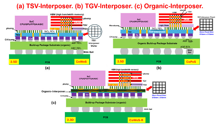
Figure 16 shows the chiplets such as the SoC and HBMs on TSV-interposer, Figure 16(a), TGV-interposer, Figure 16(b), and organic-interposer, Figure 16(c). The details comparison between these interposers are shown in Table 5.
-
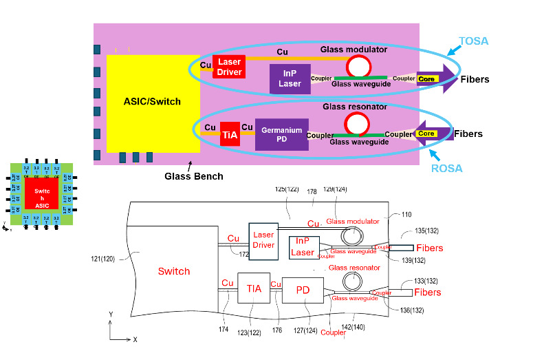
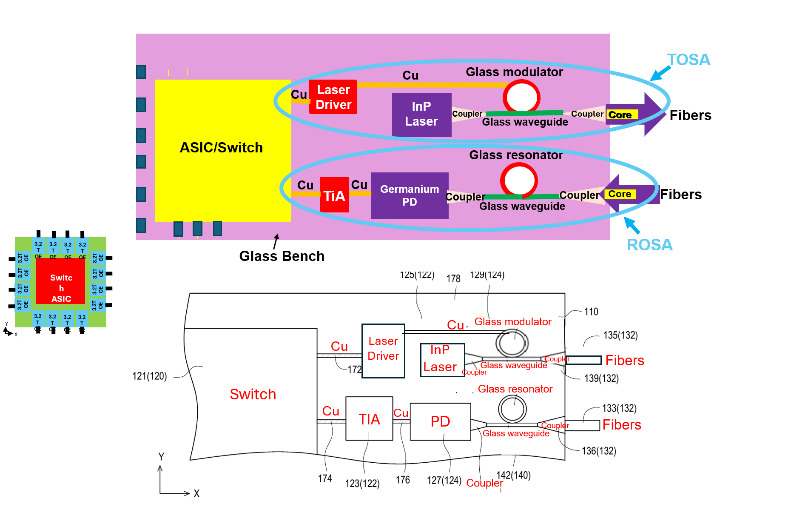
Glass packaging has a higher ability to seamlessly integrate optical/photonics interconnects. Figure 17 shows an example of co-packaged optics with glass photonics.
-
Glass packaging is a potential interconnecting (housing) method for HPC and data centers in AI era.
-
PLP has a much better area efficiency (which leads to lower costs) than WLP.
-
For HPC and data centers in AI era, the minimum pitch of the RDLs is 0.4µm and the L/S can go down to submicrons (L = S = 0.2µmmin), thus the 64nm semiconductor process is a must. The dielectric layers of the RDLs are SiO2 which are fabricated by the PECVD and the Cu metal layers of the RDLs are fabricated by dual Cu-damascene and CMP. Since the size of the glass substrate or glass interposer is very large for HPC and data centers in AI era applications, uniformity of the RDL thickness is one of the key challenges for glass packaging.
-
In the industry, large panel sizes such as 600mm x 600mm or even 700mm x 700mm have been proposed. However, among others, pick and place time is much longer, and yield/warpage are another challenge.
-
The 310mm × 310 mm format panel strikes a critical balance for HPC and data centers in AI era: it is large enough to capture the area efficiency (cost) and small enough to maintain the processing control (yield). Also, most of the successful experiences from 300mm wafer can be transferred to 310mm x 310mm panel.
-
The key advantages of glass-core substrate over the organic-core substrate are superior flatness, better dimensional stability, better heat resistance, and finer L/S RDLs.
-
The key advantages of glass TGV-interposer over the silicon TSV-interposer are better electrical isolation, flatter surface, lower Df (dissipation factor) and Dk (dielectric constant), and better area efficiency.
-
The key challenges of glass packaging are crack-free TGV formation, fine L/S = 0.2µmmin RDLs fabrication, RDLs thickness uniformity, warpage, yield, handling, testing, quality, reliability, and integration within existing manufacturing environments.